Lesson 05: General-Purpose I/O
PSoC Creator Components Datasheet: cy_pin_v2_20.pdf
The PSoC 5LP I/O system serves as the interface between the CPU core, peripheral components, and the external world. It consists of general-purpose I/O (GPIO) pins, special I/O (SIO) pins, and USBIO pins for devices with USB functionality. This flexibility allows for efficient circuit design and board layout.
PSoC 5LP I/O Types:
- GPIO (General Purpose I/O):
- Standard digital I/O pins.
- It supports analog input, CapSense, LCD drive, JTAG, and EMIF.
- Sink 8 mA, source 4 mA.
- SIO (Special I/O):
- Higher drive strength (sink 25 mA, source 4 mA).
- Hot-swap capability (5V tolerance).
- Programmable output voltage levels.
- Overvoltage tolerance up to 5.5V.
- USBIO:
- Specifically for USB 2.0 functionality.
- Source 25 mA, sink 24 mA.
5.1 GPIO (General Purpose I/O)
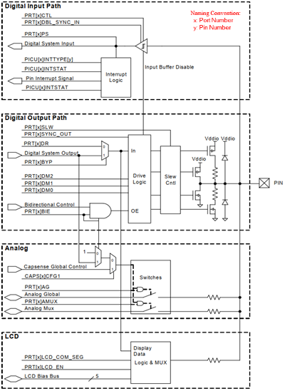
Figure 5.1: GPIO Block Diagram
Key Features:
- Pin Types: PSoC devices offer two primary pin types:
- GPIO (General Purpose Input/Output): More versatile, supporting analog I/O, LCD drive, CapSense, JTAG, higher current drive, and EMIF connectivity.
- SIO (Special I/O): Designed for specific high-speed or high-drive applications, with features like programmable drive levels and slew rates.
Common Features (Both GPIO and SIO):
- Programmable State and Drive Mode: Set initial pin states and drive modes upon device reset.
- Flexible Drive Modes: Configure output pins for various drive strengths and output types.
- Pin-Based Interrupts: Enable level-sensitive or edge-triggered interrupts on individual pins.
- Slew Rate Control: Adjust signal rise and fall times for EMI reduction or signal integrity.
- Input Thresholds: Support CMOS and low-voltage TTL input thresholds.
- Separate Read/Write Registers: Facilitate independent control of input and output operations.
- I/O Supply Grouping: Manage up to four groups of I/O pins with distinct supply voltages.
GPIO-Specific Features:
- Analog Input/Output: Use GPIO pins for analog sensing and signal generation.
- Higher Current Capability: Sink up to 8 mA and source up to 4 mA.
- LCD Drive and EMIF Support: Configure ports for LCD segment drive or EMIF address/data lines.
Functionalities:
- Digital I/O: Read digital input values and drive digital outputs.
- Interrupts: Generate interrupts based on pin state changes.
- Analog I/O (GPIO only): Interface with analog sensors or signals.
- LCD Drive (GPIO only): Control LCD segments.
- EMIF Connectivity (GPIO only): Connect to external memory interfaces.
- Peripheral Access: Interact with internal peripherals directly or through UDBs and DSI.
Port Organization:
- Groups of Up to 8 Pins: I/O pins are organized into ports, each containing up to 8 pins.
- Multiplexing: Some pins share functionality with special features like USB, debug port, or crystal oscillator.
- Control Registers: Enable special functions using dedicated control registers.
Additional Notes:
- Carefully consider pin type selection based on application requirements.
- Pay attention to multiplexed pin functions and control register settings.
5.2 Drive Modes
The PSoC 5LP GPIO (General Purpose Input/Output) pins offer a range of configurable drive modes, allowing for versatile hardware design and optimization. Here are detailed instructions on how to utilize these drive modes:
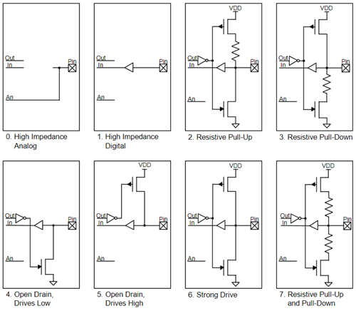
Figure 5.2: GPIO Modes
- The Out connection is driven from either the Digital System (when the Digital Output terminal is connected) or the Data Register (when the HW connection is disabled)
- The In connection drives the Pin State register and the Digital System if the Digital Inputer terminal is enabled and connected.
- The An connection connects to the Analog System.
Table 5.1: Drive Modes
| Diagram | Drive Mode | PRTxDM2 | PRTxDM1 | PRTxDM0 | PRTxDR = 1 | PRTxDR = 0 |
|---|---|---|---|---|---|---|
| 0 | High-Impedance Analog | 0 | 0 | 0 | High-Z | High-Z |
| 1 | High-Impedance Digital | 0 | 0 | 1 | High-Z | High-Z |
| 2 | Resistive Pull-Up | 0 | 1 | 0 | Res High (5KΩ) | Strong Low |
| 3 | Resistive Pull-Down | 0 | 1 | 1 | Strong High | Res Low (5KΩ) |
| 4 | Open Drain, Drive Low | 1 | 0 | 0 | High-Z | Strong Low |
| 5 | Open Drain, Drive High | 1 | 0 | 1 | Strong High | High-Z |
| 6 | Strong Drive | 1 | 1 | 0 | Strong High | Strong High |
| 7 | Resistive Pull-Up and Pull-Down | 1 | 1 | 1 | Res High (5KΩ) | Res Low (5KΩ) |
Understanding Drive Modes Configuration:
- Each GPIO and SIO pin can be individually set to one of eight drive modes.
- Drive modes are configured using three configuration bits per pin (DM[2:0]).
- These bits are set in the PRTxDM[2:0] registers.
Selecting the Drive Mode:
- Review Table 5.1, which outlines the drive state of I/O pins based on the port data register value or digital array signal in bypass mode.
- Remember, the actual I/O pin voltage is determined by both the selected drive mode and the load at the pin.
Key Considerations:
- Disable interrupts during configuration changes to avoid unexpected behavior.
- Configure all I/Os to high impedance analog modes for the lowest chip current in sleep modes or ensure pins are driven to a power supply rail by the PSoC device or external circuitry.
- Ensure that the chosen drive mode matches the intended application and external circuitry requirements.
- Understand drive mode implications: Each mode has unique characteristics that affect pin behavior and interactions with external components.
High Impedance Analog
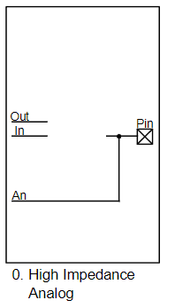
- Default reset state.
- Both the output driver and input buffer are disabled.
- Ideal for floating pins or analog signals.
- Not usable for digital input.
High Impedance Digital
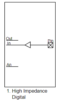
- Input buffer enabled, output driver disabled.
- Standard mode for digital inputs.
Resistive Pull-Up / Pull-Down
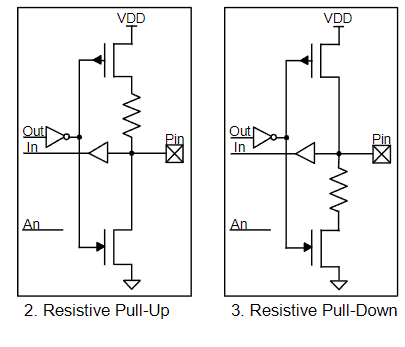
- Series resistor is in one data state, and strong drive is in the other.
- Suitable for both digital input and output.
- Commonly used with mechanical switches.
- Not available for SIO in regulated output mode.
Open Drain, Drives High / Low
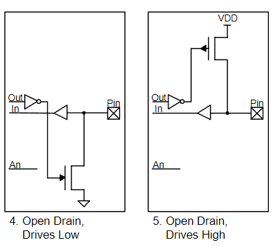
- High impedance in one data state, strong drive in the other.
- Used for both digital input and output.
- Frequently used for I2C bus signal lines (Open Drain, Drive Low).
Strong Drive
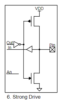
- Strong CMOS output drive in both high and low states.
- Standard mode for dedicated outputs.
- Not recommended for inputs under normal circumstances.
Resistive Pull-up and Pull-down
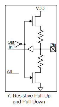
- Similar to modes 3 and 4 (Resistive Pull-Up or Pull-Down). But the pin is always in series with a resistor in this mode.
- The high data state is pull-up, and the low data state is pull-down.
- It is often used in cases where potential short circuits exist.
- Not available for SIO in regulated output mode.
5.3 Pin Configuration in PSoC Creator
Configuring the Pins Component in PSoC Creator involves several steps and considerations, ensuring that your design effectively interfaces with external signals and controls the electrical characteristics of each pin. Here's a detailed guide based on the provided information:
![]()
Basic Overview of Pin Component
- Acts as a bridge between hardware resources and physical I/O pins.
- Allows configuration of electrical characteristics (drive mode, etc.).
- It can be used with schematic wires, software, or both.
- There are four main types: Analog, Digital Input, Digital Output, and Digital Bidirectional.
When to Use a Pins Component
- Common Applications: Interfacing with external devices like potentiometers, buttons, LEDs, and sensors (e.g., proximity detectors, accelerometers).
- Usage Criterion: Whenever a design requires generating or accessing off-device signals via a physical IO pin.
Configuring Pins
- Accessing the Pins Component:
- Drag from the Component Catalog onto the schematic.
- Double-click to open the configuration dialog.
- General Settings:
- Assign physical pins (in Design-Wide Resources Pin Editor).
- Choose a contiguous or spanning configuration.
- Set display options (single pins, bus, etc.).
- Input/Output Connections:
- Select the desired functionality (analog, digital input, digital output, bidirectional).
- Configure drive modes and thresholds as needed.
- Enable output to enable hardware control of output drivers.
- Consider Vref for SIO pins with programmable or analog-routed voltages.
- Set up interrupts if required (port-dedicated or combined port interrupts).
Pins
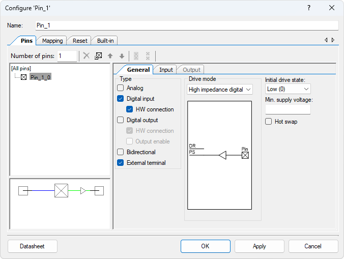
Toolbar
- Number of Pins: Set the number of device pins controlled by the Component (1 to 64, with a default of 1). Note that some configurations are limited to 8 or fewer pins if they need to be placed in a single physical port.
 Delete Pin: Removes selected pins from the tree.
 Add/Change Alias: Add or change the alias name for a selected pin. This can be done via a dialog box, double-clicking a pin, or pressing [F2].
 Move Up/Down: Adjust the order of pins in the tree.
 Pair/Unpair SIOs: Manages pairing of SIO pins, helping optimize the usage of SIO resources.
General
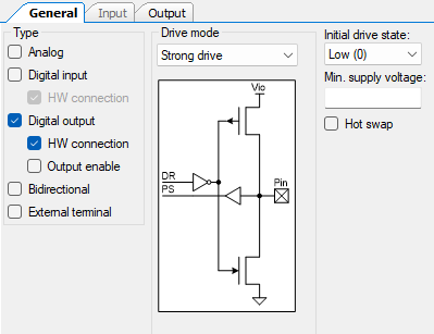
Type Selection:
- Analog: Enables the analog pin terminal for analog signal routing. Analog forces the pin to a GPIO pin.
- Digital Input: Enables the digital input pin terminal and the Input subtab for further configuration.
- The "HW Connection" parameter determines the display of the digital input terminal in the schematic.
- Digital Output: Enables the digital output pin terminal and the Output subtab.
- The "HW Connection" parameter controls the display of the digital output terminal in the schematic.
- The "Output Enable" allows for hardware signal control of the pin's output drivers.
- Bidirectional: Equivalent to enabling both Digital Input and Digital Output with HW Connection. A single bidirectional terminal is displayed instead of separate input and output terminals.
- External Terminal: Allows for connections to Off-Chip Components, illustrating external circuitry.
Drive Mode
Configuring the Drive Mode for pins in PSoC Creator is crucial to setting up your project, as it determines how each pin behaves electrically. Here are detailed instructions based on the provided information:

Drive Mode Diagram Representation
- "DR" Connection: Driven by the Digital System (if the Digital Output terminal is connected) or the Data Register (if the HW Connection is disabled).
- "PS" Connection: Drives the Pin State register and, if enabled and connected, the Digital System (for Digital Input terminal).
- Analog Connection: Directly connects to the pin.
Default Drive Modes Based on Type
- Digital Input or Digital Input:
- Default: High Impedance Digital.
- Analog:
- Default: High Impedance Analog (the only mode supporting purely Analog pins).
- Bidirectional:
- Default: Open Drain, Drives Low.
- Other Types:
- Default: Strong Drive.
Initial Drive State
- Purpose: Sets the pin's default output value after a device reset or power-on.
- Configuration:
- Choose between logic low (0) or high (1).
- Default Behavior: By default, all pins are set to logic low (0), unless changed manually or automatically configured by the pin Drive Mode parameter.
- Special Cases: For "Resistive Pull Up" and "Resistive Pull Up/Down" Drive Modes, the initial drive state is high (1) by default to activate the pull-up resistor.
- Note for PSoC 5LP Devices: This setting differs from the Power-On Reset setting under the main Reset tab, which affects the entire port's state from the moment of reset before any other device configuration.
Minimum Supply Voltage:
- Purpose: Ensures the pin is mapped to a physical pin with a supply voltage matching its output requirements.
- Voltage Source: One of the VDDIO supply inputs must provide the voltage.
- Configuration:
- Select the desired minimum voltage for high logic level output.
- Valid values are determined by the VDDIO settings in the Design-Wide Resources System Editor (in the .cydwr file) for VDDIO0/VDDIO1/VDDIO2/VDDIO3 or VDDD.
- PSoC 5LP devices with USB pins might use VDDD as the available voltage.
- Leaving this parameter blank allows placement on any pin with compatible voltage.
Hot Swap:
- Purpose: Enables a pin to tolerate voltages above its VDDIO, up to 6.0V, and prevents current leakage into the PSoC device when unpowered. Useful for connecting to unpowered communication buses like I2C.
- Configuration:
- Select Enabled to activate hot swap functionality.
- The pin must be mapped to an SIO or a GPIO Over-Voltage Tolerance (GPIO_OVT) pin.
Input
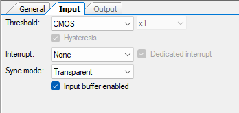
Threshold
- Purpose: Determines logic high and low voltage levels for the entire port.
- Default: "CMOS" is the default setting suitable for most applications.
- Other Options: Choose from "CMOS", "LVTTL", and various multipliers for custom interfaces.
- Multiplier Values: Choose from values like x0.4 and x0.5 to modify the threshold relative to a reference voltage (Vddio).
- SIO Requirement: SIO pins are required for Vddio, Vref, or Internal Vref (1.2V) thresholds.
- Voltage Limitations for Vref Options: Ensure the voltage stays within 1 V < (Vref x Multiplier) < (VDD - 0.4V)
- Port Contiguity: This setting affects the entire port, so ensure compatibility with other pins in the same port.
| Threshold | Allowed Multiplier values | Notes |
|---|---|---|
| CMOS | 1 | Default: Applicable for all devices |
| CMOS or LVTTL | 1 | Applicable for all devices |
| LVTTL | 1 | Applicable for all devices |
| Vddio | 0.4, 0.5 | Requires SIO |
| 0.5 x Vref | 1 | Requires SIO |
| Vref | 1 | Requires SIO |
Hysteresis:
- Improves noise immunity by adding a voltage "gap" between switching thresholds.
- Always enabled for non-SIO pins.
- Enabled or disabled for SIO pins in PSoC 5LP.
Interrupt:
- Purpose: Determines if the pin can generate an interrupt and the type of interrupt.
- Options: None (default), Rising Edge, Falling Edge, Both Edges.
- Requirement for Single Port Mapping: If interrupts are enabled, the Pins Component must be contiguous and mapped to a single physical port.
- Handling Interrupts: Use the Pin_ClearInterrupt() function to clear latched events after handling interrupts.
Dedicated Interrupt:
- Checkbox for using dedicated port interrupt logic (not capable of deep-sleep wakeup on certain devices).
- Uncheck for Combined Port Interrupt (AllPortInt) functionality for deep-sleep wakeup.
Sync Mode:
- Default Setting: Double-Sync, where input signals are synchronized to the BUS_CLK in PSoC 5LP.
- Option for Asynchronous Signals: Set to Transparent if an asynchronous signal is required and it complies with device operational requirements.
Input Buffer Enabled:
- Purpose: Enables/disables the pin's digital input buffer.
- Default Settings:
"Disabled" for Analog type pins to reduce leakage in low-power modes.
"Enabled" for all other types, including combinations with "Analog." - Power Management: Disable input buffers when not needed, especially with analog signals, to reduce power consumption.
Output
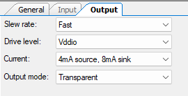
Slew Rate:
- Purpose: Controls the rise and fall rates of the pin when changing output logic levels.
- Settings:
Fast: Default setting. Use for GPIO pins with signals switching at greater than 1 MHz and for SIO pins with signals switching at greater than 10 MHz.
Slow: For signals with a switching rate less than 1 MHz (GPIO) or 10 MHz (SIO). It reduces radiated EMI (GPIO) and power usage by the SIO output buffer (SIO).
Drive Level:
- Function: Selects the output drive voltage supply sourced by the pin.
- Options:
VDDIO: Default for all pins. All pins can supply their respective VDDIO voltages.
Vref: Adhere to voltage limits - Note: PSoC 5LP resistive drive modes (Resistive Pull-Up, Resistive Pull-Down, and Resistive Pull-Up/Down )do not support Vref Drive Level.
Drive Current:
- Purpose: Determines the maximum nominal logic level current for a specific pin.
- Options:
4mA source, 8mA sink: Default.
4mA source, 25mA sink: Requires SIO. Use this for higher current requirements.
Output Mode Configuration:
- Function: Manages output signal synchronization to reduce signal skew in high-speed signals.
- Options:
Transparent: Default setting, with no synchronization.
Single-Sync: Synchronizes the output signal to the output clock (BUS_CLK on PSoC 5LP).
Mapping
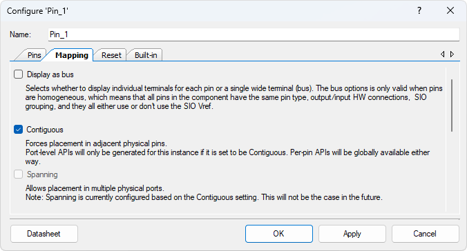
Display as Bus:
- Purpose: Determines whether to show each pin as an individual terminal or group them into a single wide terminal (bus).
- Applicability: Use this option when all pins in the Component are homogeneous, meaning they share the same:
- Pin type
- Output/input HW connections
- SIO grouping
- Usage of SIO Vref (all must use or not use the SIO Vref)
- This option is useful for saving schematic space and streamlining configuration, especially when many pins of the same type are required.
Contiguous:
- Function: Forces the placement of pins in adjacent physical positions within a port.
- Pin Placement: The actual placement depends on the device's package, as detailed in the datasheet.
- Restrictions:
When set to contiguous:- Port-level APIs are generated for the Component.
- The number of pins in the Component must be 8 or fewer.
Spanning (Indirect Control):
- Purpose: Allows the placement of pins across multiple physical ports.
- Dependency on Contiguous Setting:
- If you select contiguous, it implies non-spanning (pins are confined to a single port).
- If you select noncontiguous, it implies spanning (pins can be placed across multiple ports).
Key Points:
- Homogeneous pins can be grouped into a bus for convenience.
- Contiguous placement is necessary for port-level APIs and has pin count restrictions.
- Spanning placement is achieved by disabling contiguity.
- Consider these options carefully based on your application's requirements and schematic layout preferences.
Reset
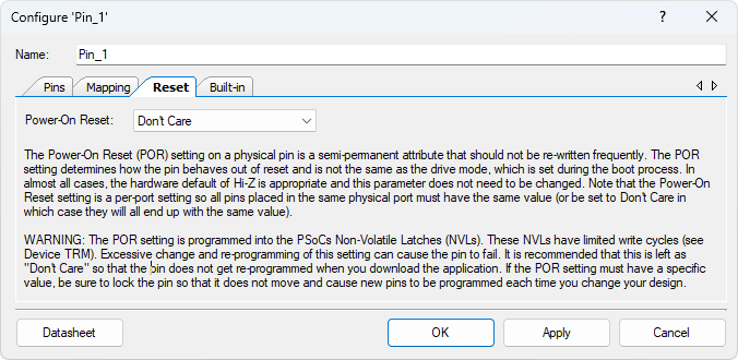
Power-On Reset (POR):
- POR determines the initial state of a pin upon device power-up.
- It is distinct from the drive mode set during the boot process.
- POR is a per-port setting, meaning all pins within a physical port must have the same POR value.
Default Setting: The default POR is "Don't Care", which means:
- If all pins in the port are "Don't Care", the device's default POR (Hi-Z Analog) is used.
- If any pins in the port have a specific POR set, that value applies to all "Don't Care" pins in the port.
POR Options:
- High-Z Analog: Pin becomes high-impedance input upon reset.
- Pulled-Up: The pin is weakly pulled high upon reset.
- Pulled-Down: The pin is weakly pulled low upon reset.
Warning and Recommendations:
- Avoid changing POR settings frequently, as excessive programming can wear out PSoC's Non-Volatile Latches (NVLs).
- If a specific POR value is essential, lock the pin to prevent unintended reprogramming.
- PSoC Creator usually sets POR appropriately based on pin type and configuration.
- Only modify POR if you have specific requirements and understand the implications.
Note restrictions:
- Resistive drive modes (Resistive Pull Up, Resistive Pull Down, Resistive Pull Up/Down) cannot use Vref for output Drive Level.
- Over Voltage Tolerance:
To ensure proper over-voltage tolerance, use one of these Drive Modes:- High Impedance Analog
- High Impedance Digital
- Open Drain, Drives Low
- PSoC 5LP USBIO Pins:
- Support only "Open Drain, Drives Low" and "Strong Drive" modes.
- For using USBIO pins as inputs, choose "Open Drain, Drives Low".