Lab 09: Exclusive-OR Circuits and Parity
Objective
- Understand and implement XOR (exclusive-OR) gates in digital circuits.
- Design circuits that utilize XOR gates for parity generation and checking.
- Learn how parity is used to detect transmission errors in binary data.
- Construct and test an XOR-based parity generator and checker circuit.
- Simulate transmission errors and observe the behavior of the parity checker.
- Demonstrate error detection limits in a practical XOR circuit setup.
Required Reading Materials
- Textbook: Digital Design: with an introduction to the Verilog HDL, 5th edition, Mano and Ciletti, ISBN-13: 978-0-13-277420-8
Chapters 3 and 4 - Datasheet: 7486
Components Required
| Component/Device | Description | Quantity |
|---|---|---|
 |
Breadboard | × 1 |
| Green LED | × 4 | |
| Red LED | × 1 | |
| 220 Ω (red red brn gld) | × 5 | |
| 7486 Quad 2-input XOR | × 3 | |
| Digilent Analog Discovery 2 (AD2) or Analog Devices: ADALM1000 (M1K) |
× 1 |
Experiments
Every experiment section that requires you to build a circuit and test it has an asterisk (*). For those sections:
- For the in-class lab: Demonstrate the working circuit to your lab instructor.
- For online lab: Take a video to describe your circuit, upload the video to YouTube, and put the link in the report.
Exp #9.1 ALL-XOR Circuit
For ease of use, we replace the exclusive-or symbol ⊕ in the following discussion with the keyboard symbol ^. This is common practice in software packages designed for programmable logic devices (PALs, PLDs, etc.).
An all-XOR function has the form F(A,B,C,D...) = A ^ B ^ C ^ D ^ …. At any given time, some of the inputs will be 1's, the others 0's; e.g. 01110110 for an 8-input function. If we group the 1's and 0's separately and then pair them, we get 0(00)(11)(11)1. This pattern has odd parity (an odd number of 1's).
Now, the XOR of 2 bits is 0 if they are equal (00 or 11), and 1 if they are not (01 or 10). Thus, if we XOR the paired 1's and 0's in 0(00)(11)(11)1, we get 0(0)(0)(0)1. Pairing the 0's, we can rewrite this as (00)(00)1 and again XOR the pairs. The result is F = 0^0^1 = 0^1 = 1. If the extra 1 had instead been a 0, the result would have been F = 0^0 = 0.
This will be true in general, regardless of how many inputs there are. If input parity is odd, there is an extra 1 that can't be paired off. The result is always F = 1. For even parity, it is always F = 0. Because of this property, XORs are used in circuits that recognize input parity; i.e. parity generators and checkers.
Exp #9.2 * Parity Generating and Checking Circuits using XORs
Using parity is a low-cost method for detecting errors when transmitting binary data in a noisy environment (electromagnetic noise). An error can cause one or more bits of data to change their value. For example, assume that a 7-bit ASCII text character is being transmitted from sender to receiver. Assume the character being sent is the letter 'A'. The 7-bit ASCII code for 'A' is 1000001. During transmission, assume that an error occurs causing the last bit to change from a 1 to a 0.
The data being received would be 1000000 which is the '@' character, not the A. Parity can be used to detect that type of error so that the receiver knows that the data is incorrect.
Parity is based on the number of ones in the data to be transmitted; the data's parity is said to be even if the data has an even number of ones; otherwise, parity is odd. The sender adds a parity bit to the data using a parity generator so that the transmitted combination (parity bit plus data) has the kind of parity the receiver expects. If the receiver expects the combination to have even parity but the data has odd parity, the sender adds a parity-bit of one; if the data has even parity, it adds a zero. Either way, the transmitted combination must have an even number of ones. The opposite is true if the receiver expects odd parity.
Consider the above example where the data is the 7-bit ASCII character 'A'. Suppose the sender and receiver are using an even parity system. If a parity bit is placed at the left of the data, then the 8-bit combination transmitted is 01000001. The parity bit is a zero since the data has two ones which are already an even number of ones. If the same error occurs in transmission, the data received will be 01000000. At the receiver, a parity checker checks the number of ones to make sure the received combination has the correct parity (in this case, even). For this example, the parity checker will detect that there is an odd number of ones (only one 1) and flag an error: C = 1, where C is the error indicator. A system like this cannot detect all errors as you'll discover in this experiment nor can it correct the error. But with only one added bit, it can detect a large number of errors. More sophisticated error-correcting codes can be used if errors need to be corrected.
Drawing and Building the circuit
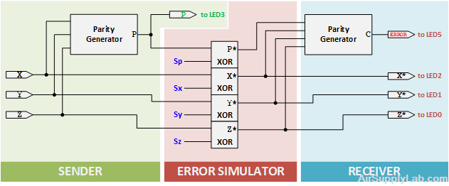
Using Express SCH, draw the following sender-receiver circuit. Design it to use EVEN parity. Replace the Parity Generator and Checker boxes with appropriate XOR circuits. Also, show the Error Simulator as 4 XOR gates (this part is discussed on the next page). Your diagram will consist of nothing but 7486 XOR gates from 3 chips. Be sure to include U numbers so you will know which gates come from which chip.

Figure 9.1: Even Parity Checking Circuit
In your diagram, show X, Y, Z, and Error Simulator inputs, Sp, Sx, Sy, and Sz, with input port symbols. Same for X*, Y*, and Z*, but with output port symbols. (See port symbols for X and X* in the diagram.) No need for an output port symbol for C since it connects directly to an LED. (To find the LED symbol using KiCad, go to the "Library components" listing, click on the Find button, and type in "Semiconductor - LED"; i.e. Semiconductor (space) hyphen (space) LED. )
Since PXYZ patterns are to be sent with EVEN parity, the parity generator will examine the input pattern XYZ and output P = 1 if the pattern has the wrong parity (ODD), and P = 0 otherwise. Thus, if inputs XYZ = 100 (odd parity), then P = 1. The transmitted pattern will be PXYZ = 1100, with even parity as required. Likewise, the parity checker also examines its input pattern (in this case P*, X*, Y*, Z*) and outputs C = 1 if the pattern has the wrong (ODD) parity, and C = 0 otherwise. Both parity generator and parity checker circuits are to be designed with XORs only. Include your circuit diagram in your lab journal.
It is possible for one or more errors to enter the bit pattern as it travels the distance from the sender to the receiver. (This distance might be only a few centimeters or it might be many miles.) The effect of such errors on the parity checker can be demonstrated by means of the Error Simulator.
The Error-Simulator circuit consists of 4 XOR gates used as selectable inverters. Each has a data input and a select input, S. When S = 1, the data bit is complemented; otherwise, it is unchanged. Thus, P* = P if Sp = 1, but P* = P if Sp = 0. (See Lab 08 for another example of selectable inverters.)
The following truth table shows how XOR gates can be used as selectable inverters: P* = SP ⊕ P
| SP | P | P* | |
|---|---|---|---|
| 0 | 0 | 0 | if SP = 0, P* = P |
| 0 | 1 | 1 | |
| 1 | 0 | 1 | if SP = 1, P* = P |
| 1 | 1 | 0 |
Connect XYZ to three switches and connect the S inputs to four switches, as indicated in the circuit diagram. Test your circuit with all S inputs initially at 0. This simulates normal conditions where patterns are transmitted without error; i.e. P* = P, X* = X, etc.. For each of the 8 patterns of XYZ (000-111) observe the LEDs for P and C. Whenever XYZ has odd (wrong) parity (e.g. XYZ = 010), the parity generator should output P = 1 so transmitted parity is even (1010). Otherwise, P = 0. C should be 'low' all the time, indicating no errors. (Enter your observations into the following table for this test and paste them into your lab report.)
Table 9.1: Parity Check Generator
| Sender | Parity Check | ||
| Data Switches |
(even) | ||
| X | Y | Z | PLED |
| 0 | 0 | 0 | |
| 0 | 0 | 1 | |
| 0 | 1 | 0 | |
| 0 | 1 | 1 | |
| 1 | 0 | 0 | |
| 1 | 0 | 1 | |
| 1 | 1 | 0 | |
| 1 | 1 | 1 | |
Now, introduce an error by setting Sz to logic-1. This inverts Z* and gives the received pattern the wrong parity. C responds by going high (error). Make sure this happens in your circuit for all XYZ values. Next, set Sy = Sz = 1. Note that C goes low, indicating no error when there actually are two.
Now, set Sx = Sy = Sz = 1. This should bring C high again. Finally, with all four S's high, C goes low once more, even though there are now 4 errors! You can see the limitation of this sort of parity system. It only works reliably if the probability of more than 1 error is very low. Then the chance of 2 or 4 errors is vanishingly small, making it extremely unlikely that C will give a false indication.
Enter your test results into the following table and copy them into your report.
Table 9.2: Circuit Results for Error Detection
| Sender | Data transmission | Receiver | |||||||||
| Data Switches |
LED | Error Simulator | LED | ||||||||
| X | Y | Z | P | SP | SX | SY | SZ | Cerror | X* | Y* | Z* |
| 0 | 0 | 0 | 0 | ||||||||
| 0 | 0 | 0 | 1 | ||||||||
| 0 | 0 | 1 | 1 | ||||||||
| 0 | 1 | 1 | 1 | ||||||||
| 1 | 1 | 1 | 1 | ||||||||
| 1 | 0 | 0 | 0 | ||||||||
| 1 | 0 | 0 | 1 | ||||||||
| 1 | 1 | 1 | 0 | ||||||||
| 1 | 1 | 0 | 1 | ||||||||
