Lab 08: Adder and Subtractors
Objective
- Design a 4-bit binary adder and subtractor using the 7483 IC.
- Learn how to modify an adder to function as a subtractor using 2's complement.
- Build and test the circuit for both addition and subtraction of 4-bit numbers.
- Analyze the circuit outputs, including carry and borrow results.
- Use the circuit as a comparator to determine if one number is greater than, equal to, or less than another.
Required Reading Materials
- Textbook: Digital Design: with an introduction to the Verilog HDL, 5th edition, Mano and Ciletti, ISBN-13: 978-0-13-277420-8
Chapter 2 Sec. 4-5 - Datasheet: 7400, 7402, 7404, 7408, 7432, 7483, 7486
Components Required
| Component/Device | Description | Quantity |
|---|---|---|
| 7400 Quad 2-Input NAND | × 1 | |
| 7402 Quad 2-Input NOR | × 1 | |
| 7404 Hex Inverter | × 1 | |
| 7408 Quad 2-Input AND | × 1 | |
| 7432 Quad 2-Input OR | × 1 | |
| 7483 4-Bit Binary Full Adder | × 1 | |
| 7486 Quad 2-Input XOR | × 1 |
Experiments
Every experiment section that requires you to build a circuit and test it has an asterisk (*). For those sections:
- For the in-class lab: Demonstrate the working circuit to your lab instructor.
- For online lab: Take a video to describe your circuit, upload the video to YouTube, and put the link in the report.
Exp #8.1 Design Full Adder and Subtractor
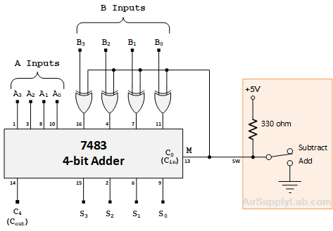
The 7483 is a 4-bit parallel adder. It consists of a chain (or "cascade") of 4 full-adder circuits. A subtractor equivalent of the 7483 could similarly be created by cascading four 1-bit full-subtractor circuits.
A full subtractor has a truth table very much like that of a full adder. Its outputs are a different bit and a borrow bit. With four of these chained together to produce a true 4-bit subtractor, you could generate the difference between two numbers, (A3…A0) and (B3…B0), as well as a borrow-out. If A < B, the borrow-out would be high.
Such a subtractor chip is not available, probably because it is easy enough to modify the 7483 so that it also subtracts. With this circuit, "subtraction" is done by 2's-complement addition.
A select input M (for Minus) is brought to the 7483- based adder/subtractor circuit from a toggle switch. It determines whether input B is added to or subtracted from input A. When M is 0, the circuit adds; when
M = 1, it subtracts.
C4 is the adder's carry-out bit. The 4-bit output is S = (S3..S0). It stands for sum when adding, but when subtracting, it represents the difference. In other words:
- When M = 0, output S = (A3 … A0) + (B3 … B0) + 0
- When M = 1, output S = (A3 … A0) + (B3 … B0) + 1
The 0 and 1 at the right are from the 7483's carry input, C0 (Cin) which is connected to M. In the second expression above, M complements the B inputs and adds the 1. The result is A + (B + 1) = A - B. Complementing each Bn is done with an XOR controlled by M: if (M == 0), output = Bn; if (M == 1) , output = Bn.
Question
- Use the KiCad to draw the Circuit Diagram as shown in Figure 8.1.
Exp #8.2 * Build Adder/Subtractor
Build the adder/subtractor described in Exp #8.1.
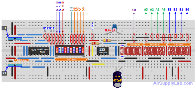
- Let the A's come from one 4-switch block and the B's from another.
- C0 connects to one switch.
- S0 ~ S3 connects to LED0 ~ LED3.
- C4 connects to LED4.
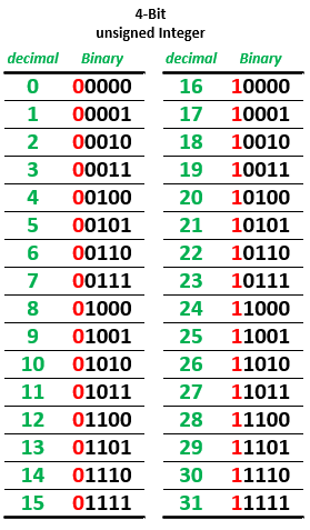
First, slide the switch connected with C0 to the down position (Co = 0) to set the circuit as a 4-bit binary adder, then test it by adding two pairs of 4-bit numbers. One pair should produce a sum that is within the range of a 4-bit unsigned number (sum ≦ 15). The other set should produce a sum that is outside the range of a 4-bit number. Record the values used and the resulting outputs, including the carry-out. In your lab notebook, compare your results with hand calculations using binary addition. Based on your observations, note what is the significance of the carry-out from the adder?
Table 8-1: Adder
| Input Values | Hand Calculation | Results from Adder | ||||
|---|---|---|---|---|---|---|
| A | B | A + B | Cout | S3 S2 S1 S0 | ||
| A + B ≦ 15 | Decimal | C4 | ( )LED | |||
| Binary | ( )2 | ( )2 | ( )2 | |||
| A + B > 15 | Decimal | C4 | ( )LED | |||
| Binary | ( )2 | ( )2 | ( )2 | |||

Now, slide the switch connected with C0 to the up position (Co = 1) to set the circuit as a 4-bit binary subtractor,
Then subtract using several different values of A and B. When performing subtraction, include all 3 cases:
- A > B
- A = B
- A < B
Record the values used and the resulting outputs, including the carry-out. In your lab journal, compare your results with hand calculations using 2's-complement addition for subtracting. Also, for each case, what is the relationship between the carry-out generated by this circuit with the borrow that would be generated by a true subtractor? You will need to know this for Exp #8.3.
Complete the table below by selecting two positive values that match the requirements in each field. Calculate the results manually in the Hand Calculation field. Enter the A and B values on the switches, and record the LED results in the table.
Table 8-2: Subtractor
| Relationship | Input Values | Hand Calculation | Results from Subtractor | |||
|---|---|---|---|---|---|---|
| A | B | A - B | Cout | S3 S2 S1 S0 | ||
| A > B | Decimal | |||||
| Binary | ( )2 | ( )2 | C4 | ( )LED | ||
| Decimal | ||||||
| Binary | ( )2 | ( )2 | C4 | ( )LED | ||
| Decimal | ||||||
| Binary | ( )2 | ( )2 | C4 | ( )LED | ||
| A = B | Decimal | |||||
| Binary | ( )2 | ( )2 | C4 | ( )LED | ||
| Decimal | ||||||
| Binary | ( )2 | ( )2 | C4 | ( )LED | ||
| A < B | Decimal | |||||
| Binary | ( )2 | ( )2 | C4 | ( )LED | ||
| Decimal | ||||||
| Binary | ( )2 | ( )2 | C4 | ( )LED | ||
| Decimal | ||||||
| Binary | ( )2 | ( )2 | C4 | ( )LED | ||

Exp #8.3 * 4-bit Comparator
Do not unplug your Adder/Subtractor circuit, you will still need it for this experiment.
The circuit of Exp #8.2, configured as a subtractor, can be used to compare two 4-bit numbers. Subtractor outputs Cout and (S3…S0) can be combined logically to indicate the relationship between inputs A and B. The gate circuit needed to do this appears as the interface block in the following diagram.

Figure 8.2: 4-bit Comparator
Design the contents of this interface. You will build the circuit using only 2 chips:
- a 7402 NOR chip
- either a 7432 OR chip or a 7408 AND chip.
Design the interface in two ways: (a) an OR and NOR circuit, and (b), a NOR and AND circuit. Include both designs in your lab journal and build and test one of them. Each design consists of 3 parts — one for each output — and requires 5 gates total. KiCad has custom DM symbols for all gates (including ANDs and ORs). Use them, but only where they make circuit logic easy to follow (i.e. where bubbles cancel).
For each design:
- Start by drawing the circuit to generate "A = B". This output is true only when A - B = 0; i.e. only when (S3…S0) = 0000. Therefore, for this part of the interface block, you must combine inputs S3…S0 using gates so that output "A = B" goes high when S3…S0 are all low. A 4-input NOR would be the perfect solution — if one were available. Instead, you will have to do the design with the gates assigned.
- Next, draw the circuit to generate output "A < B". This output is true if a borrow results when subtracting B from A. With a true subtractor, you would just connect "A < B" to the borrow bit. However, the "subtractor" used here is really a 2's-complement adder, so it produces a carry-out instead of borrowing. Therefore you must use the relationship between carry-out and borrowing observed in Section 8.2
- Finally, draw the circuit for "A > B". This output goes high when the other two are low, since "A > B" is true only when "A = B" and "A < B" are both false.
Again: use DeMorgan gate symbols wherever they contribute to making circuit logic clear.
Question
- Implement your design in hardware based on your group number..
$Group\# = \left\{ {\matrix{
{Odd} & { \Rightarrow {\rm{Build\;NOR + OR\;circuit}}\,} \cr
{Even} & { \Rightarrow {\rm{Build\;NOR + AND\;circuit}}} \cr} } \right.$
Build the circuit and connect it to the subtractor outputs, then test it for these three cases:
A = B, A < B, and A > B. (You pick A and B values from Exp #8.2 Table 8-2). Demonstrate your results to your instructor.
In your lab report, present a clear discussion of the following based on your lab results:- If (A = B), what are subtractor outputs S3…S0, and C4? Explain why output "A = B" goes high.
- If (A < B), what are S3…S0, and C4? Explain why output "A < B" goes high.
- If (A > B), what are S3…S0, and C4? Explain why output "A > B" goes high.
Reminder: Refer to the section in case you get stuck trying to debug your circuit.

