KB 03: Intel FPGA M9K Embedded Memory Blocks
The M9K memories are Intel/Altera's embedded high-density memory arrays. Nearly all modern FPGAs include something similar to varying sizes. In Xilinx FPGA, it is called "BlockRAM." Each M9K block is useful for storing processor code, implementing lookup schemes, and implementing large memory applications. Each M9K memory block provides 256 × 36 RAM blocks, which contains 9216 programable bits, including parity bits (or 8,192 bits without parity bits) and is capable of very highly flexible port configurations.
In the MAX10 device, the M9K is a synchronous memory and can operate at up to 284 MHz. The following table lists the configuration sizes for the M9K memory block:
| Operating Modes | Port Widths |
|---|---|
| Single port | ×1, ×2, ×4, ×8, ×9, ×16, ×18, ×32, and ×36 |
| Simple dual-port | ×1, ×2, ×4, ×8, ×9, ×16, ×18, ×32, and ×36 |
| True dual-port | ×1, ×2, ×4, ×8, ×9, ×16, and ×18 |
| Number of words (words) | Number of bits in words (bits) |
|---|---|
| 8192 | 1 |
| 4096 | 2 |
| 2048 | 4 |
| 1024 | 8 or 9 |
| 512 | 16 or 18 |
| 256 | 32 or 36 |
In general, embedded memories will perform much better than memories synthesized from LUTs:
- Higher clock rates / higher throughput / lower latency
- Lower energy dissipation
- Lower use of chip resources
- Exception: very small memories
M9K Overview
The MAX10 embedded memory block is optimized for applications such as high throughput packet processing, embedded processor program, and embedded data storage. MAX10 embedded memory supports the following general features:
- Each M9K memory block supports two clock-enable controls, which allows each input register and core memory cell to use either clock-enable controls or no gating clock control. The output register supports one clock-enable control or no gating clock control.
- The Write Enable (WE) and Read Enable (RE) controls are independent in M9K memory blocks. Independent WE (write-enable) and RE (read-enable) controls allow you to reduce power consumption under circumstances when data output during a write operation is not critical.
- Packet mode in which the M9K memory block is split into two 4.5K single-port RAMs.
- Byte enables for data input masking during writes.
- Two clock-enable control signals for each port (port A and port B).
- Initialization file to preload memory content in RAM and ROM modes.
The MAX 10 embedded memory structure consists of 9,216-bit (including parity bits) blocks. You can use each M9K block in different widths and configurations to provide various memory functions such as RAM, ROM, shift registers, and FIFO. The following lists are M9K interface modes:
| Memory Operation Mode | Related IP Core | Description |
|---|---|---|
| Single-port RAM | RAM: 1-PORT IP Core | The single-port mode supports non-simultaneous read and write operations from a single address. Use the read enable the port to control the RAM output ports behavior during a write operation:
|
| Simple dual-port RAM | RAM: 2-PORT IP Core | You can simultaneously perform one read and one write operations to different locations where the write operation happens on Port A and the read operation happens on Port B. In this memory mode, the M9K memory blocks support separate we and re signals. To save power, keep re signal low (inactive) when not reading. |
| True dual-port RAM | RAM: 2-PORT IP Core | You can perform any combination of two-port operations:
|
| Single-port ROM | ROM: 1-PORT IP Core | Only one address port is available for read operation. You can use the memory blocks as a ROM.
|
| Dual-port ROM | ROM: 2-PORT IP Core | The dual-port ROM has almost similar functional ports as single-port ROM. The difference is dual-port ROM has an additional address port for read operation. You can use the memory blocks as a ROM.
|
| Shift-register | Shift Register (RAM-based) IP Core | You can use the memory blocks as a shift-register block to save logic cells and routing resources. The input data width (w), the length of the taps (m), and the number of taps (n) determine the size of a shift register (w × m × n). The size of the shift register must be less than or equal to the maximum number of memory bits (9,216 bits). The size of (w × n) must be less than or equal to the maximum of width of the blocks (36 bits). You can cascade memory blocks to implement larger shift registers. |
| FIFO | FIFO IP Core | You can use the memory blocks as FIFO buffers.
|
| Memory-based multiplier | ALTMEMMULT IP Core | You can use the memory blocks as a memory-based multiplier. |
You can use a Memory Initialization File (.mif) or Hexadecimal (Intel-Format) File (.hex) to preload the memory contents when the M9K memory block is configured as a RAM, ROM, or MLAB. All RAM instances are kept in the form of block RAM until after analysis and synthesis, when the Fitter converts block RAM to MLABs to balance out the resource usage, or if the design specifies MLAB.
Main Methods to Specify an M9K Memory Blocks
There are four methods to specify an M9K memory block:
- Let Quartus Prime infer an M9K from appropriate Verilog (generally the best approach).
- Use the IP catalog tool (see an example in the PLL Tutorial)
- Use Quartus QSYS (not recommended)
- Use a Quartus "Language Template"
- Edit ➤ Insert Template ➤ Verilog ➤ Full Designs ➤ RAMs and ROMs
- See the Compilation Report to find out if M9K blocks were really used during synthesis.
Memory Initialization Capabilities
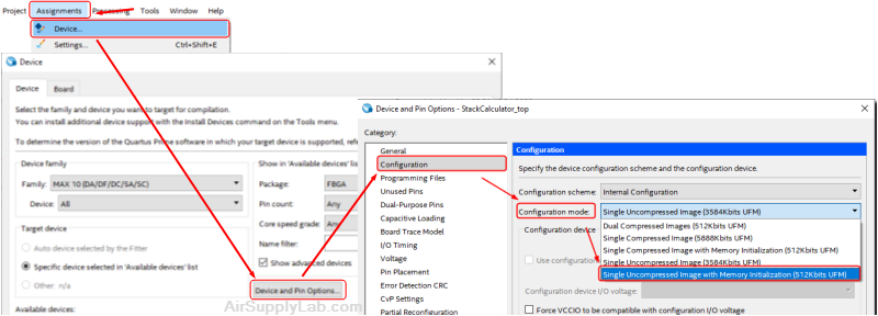
To properly initialize the M9K memory blocks, the Quartus Prime must be set up to include memory initialization data with the device's programming data (bitstream) by following these steps in Quartus before compiling:
- Click Assignments ➤ Device... from the main menu
- Click Device and Pin Options... button
- Go to the Configuration tab
- From the Configuration Mode drop-down, select Single Uncompressed Image with Memory Initialization. (typically Quartus is not set to use memory initialization by default)

Figure 1: Configuration for Using M9K Memory Initialization
- ROMs – The embedded memory array is truly an SRAM acting like a ROM so its contents must be initialized.
- SRAM – Unique to FPGAs, the contents of SRAMs may be initialized at configuration time.
- Contents are specified in Verilog in an initial block. This is the only time you may synthesize an initial block!
- Initialization data contents are specified with a .mif file by Quartus
Once you create an M9K memory block, you can specify an initialization file in Quartus Prime, meaning that your memory could be populated at reset. A common way to provide init data is through a .mif file.
Memory Initialization File (.mif)
An ASCII text file (with the extension .mif) that specifies the initial content of a memory block (CAM, RAM, or ROM), that is, the initial values for each address. This file is used during project compilation and/or simulation.
A Memory Initialization File (MIF) is used as an input file for memory initialization in the Compiler and Simulator. You can also use a Hexadecimal (Intel-Format) File (.hex) to provide memory initialization data.
A MIF contains the initial values for each address in the memory. A separate file is required for each memory block. In a MIF, you must specify the memory depth and width values. In addition, you can specify data radixes as binary (BIN), hexadecimal (HEX), octal (OCT), signed decimal (DEC), or unsigned decimal (UNS) to display and interpret addresses and data values. Data values must match the specified data radix.
Following is a sample MIF:
% multiple-line comment
multiple-line comment %
-- single-line comment
DEPTH = 32; % Memory depth and width are required %
% DEPTH is the number of addresses %
WIDTH = 14; % WIDTH is the number of bits of data per word %
% DEPTH and WIDTH should be entered as decimal numbers %
ADDRESS_RADIX = HEX; % Address and value radixes are required %
DATA_RADIX = HEX; % Enter BIN, DEC, HEX, OCT, or UNS; unless %
% otherwise specified, radixes = HEX %
-- Specify values for addresses, which can be single address or range
CONTENT BEGIN
[0..F]: 3FFF; % Range--Every address from 0 to F = 3FFF %
6 : F; % Single address--Address 6 = F %
8 : F E 5; % Range starting from specific address %
% Addr[8] = F, Addr[9] = E, Addr[A] = 5 %
--
END;
- If multiple values are specified for the same address, only the last value is used.
- You can create a Memory Initialization File in the Memory Editor, the In-System Memory Content Editor, or the Quartus Prime Text Editor.
For more information, use Quartus Help and search for the topic "Memory Initialization File".
On-Chip Memory Array in MAX10 FPGA
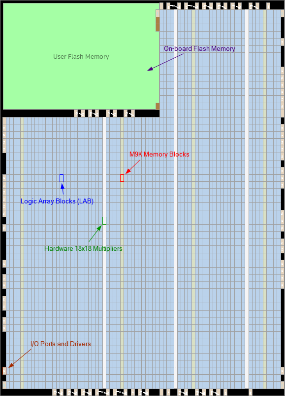
The DE10-Lite FPGA chip (10M50DAF484C7G) as shown in below:

- Yellow rectangles are M9K memory blocks
- 182 blocks on each chip
- Total of 182 KBytes (204 KB)
- Light-blue rectangles: Logic Array Blocks (LAB), each of which contains 16 logic elements (LE), each of which contains a 4-input LUT, a flip-flop, and routing muxes
- White rectangles: hardware 18x18 multipliers
- Green rectangle: on-board flash memory that can store the bit-stream that programs the FPGA when it is powered on
- Brown blocks on the border are I/O ports and drivers
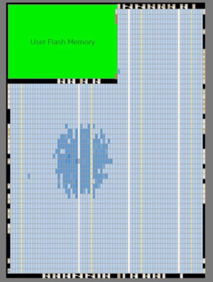
Example 1: Utilizing LUT-Memory

- In this example, the M9Ks are not enabled and the large ROM memories are implemented using individual Logic Elements
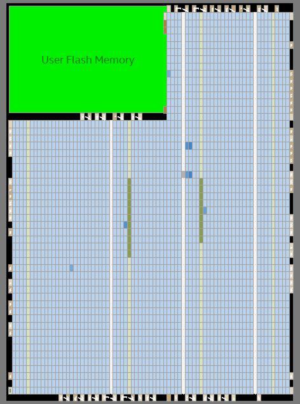
Example 2: Utilizing BlockRAM Memory (M9K)

- In this example, the M9K memory blocks are enabled.
- Many logic elements are freed for other uses.
- Should have a higher maximum clock frequency
- Should dissipate lower power