Lesson 01: Create a New FPGA Project using Quartus Prime Standard
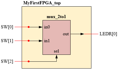
This tutorial will teach you how to create an FPGA design and test the design by using Altera Quartus Prime software. Let us create an FPGA project for 2-to1 Multiplexer using Verilog HDL.
1. Creating a Project
Creating a Project
You can create a new project by clicking New Quartus Prime Project on the File ➤ New... menu. When creating a new project, you specify the working directory for the project, assign the project name, and designate the name of the top-level design entity. You can also specify which design files, other source files, user libraries, and EDA tools you want to use in the project, as well as the target device.
- Launch Quartus (Quartus Prime 25.x) Lite (or Standard) Edition
There should be a desktop icon. Otherwise, search through the Windows Start menu to find it.
- Start the New Project Wizard
In the Quartus Prime window, click on the menu File ➤ New..., select on Quartus Prime Project, then click on the OK button.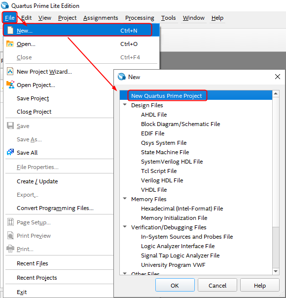
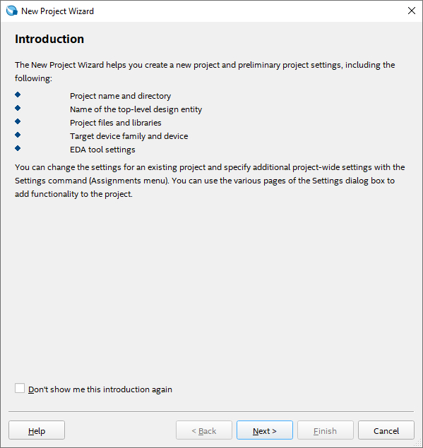
- Next, the Introduction page opens. Click on the Next button.
- Select the Working Directory, Project Name, and Top-Level Design Entity Name
On the next screen, enter a directory where you will store your Quartus Prime project files for this design, for example, R:\Project\EE4480\MyFirstFPGA.
Enter the project name, type MyFirstFPGA.
Enter the name of the top-level design entity for this project. By default, this name matches the project name. Here, I recommend adding "_top" to the name so you can easily recognize the top-level module file. Here, you can type MyFirstFPGA_top.
Click Next.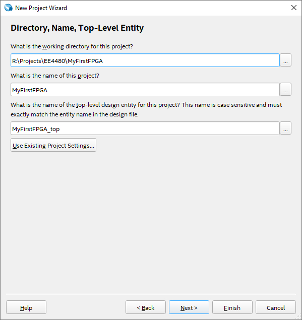
Note: A window may pop up stating that the chosen working directory does not exist. Click Yes to create it.
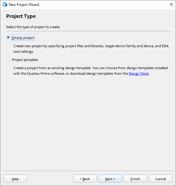
Don't use any space or special characters in the file or project names. Use an underscore ( _ ) if you need to put a space in your file or project name. - Next, select the project type. Please select the Empty project, then click on the Next button.
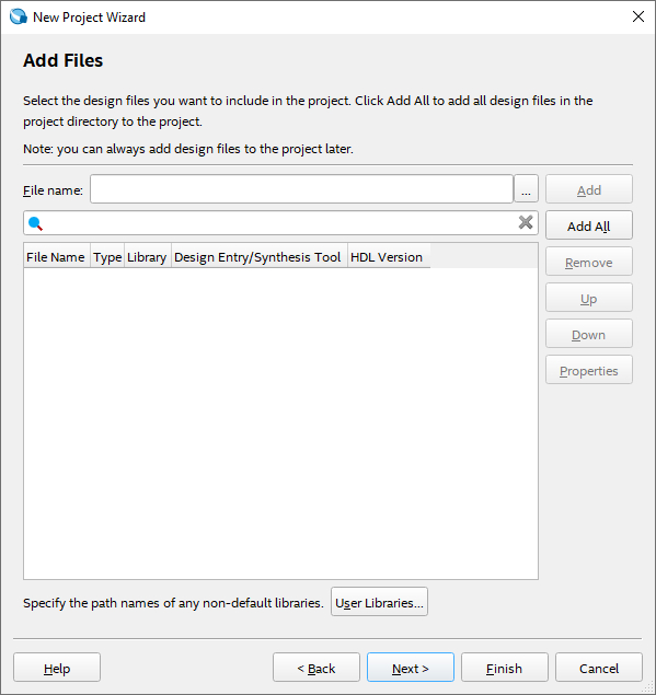
- In the next dialog, click Next again as we will not be adding any preexisting design files at this time.
- Select the Family and Device Settings
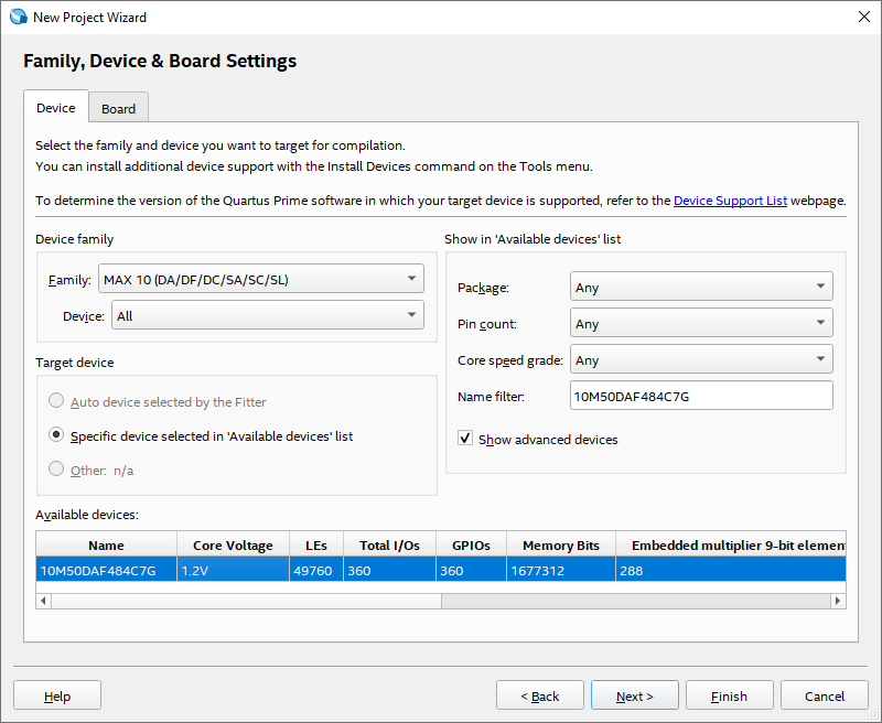
Select the family and device you used for this project, then click on the Next button.
- From the pull-down menu labeled Device family, select MAX 10(DA/DF/DC/SA/SC).
- In the list of available devices:
- If you are using terasIC DE10-Lite Board, please select 10M50DAF484C7G device.
- If you are using Arrow BeMicro MAX 10 Evaluation Kit Board, please select 10M08DAF484C8GES device.
- Click Next
- Select simulation tool:
- For 20.1 or newer versions:
In the EDA Tool Settings dialog, select Simulation to Questa Altera FPGA, and Format(s) to Verilog HDL. Then click Next.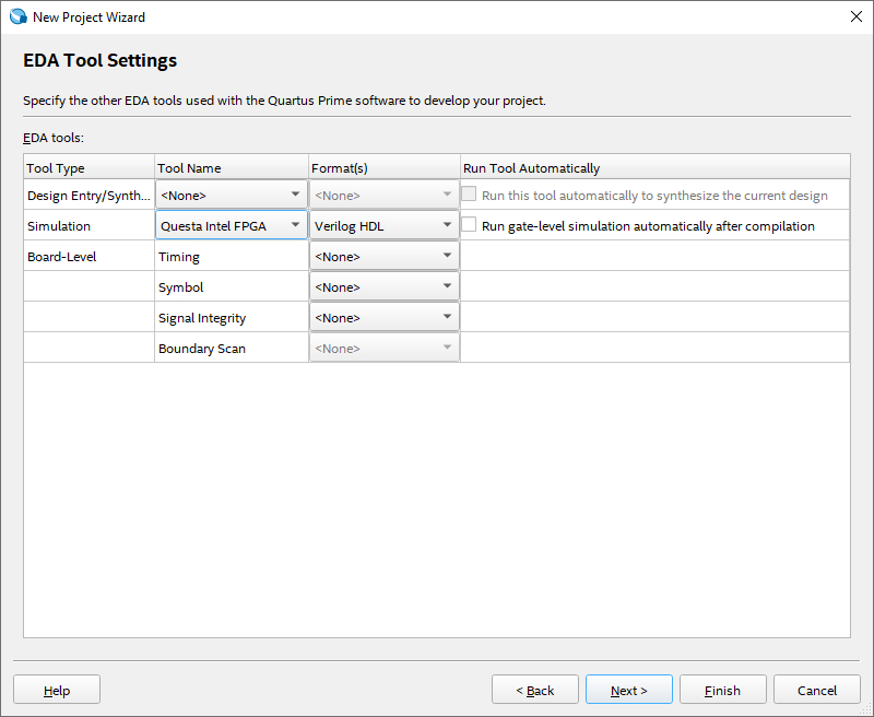
- For 20.0.1 or previous version:
In the EDA Tool Settings dialog, select Simulation Tool Name to ModelSim-Altera, and Format(s) to Verilog HDL. Then click Next.
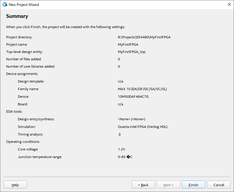
- For 20.1 or newer versions:
- Finally, the New Project Wizard will show you a summary of this project. Click Finish to complete the New Project Wizard.
2. Create Top-Level Design and 2-to-1 MUX
Create Top-Level Design and 2-to-1 MUX
After creating the project file, the next step is to enter the design phase. In this phase, you create a Verilog HDL (.v) file that serves as the top-level design.
In Quartus, the top-level module must have the same name as the top-level design entity name you entered in the New Project Wizard window and must be in a file with the same name and a ".v" extension.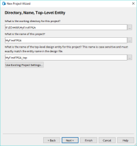
- Creating the top-level module goes back to the main Quartus Prime window:
Select File ➤ New... from the Menu bar.
Select the Verilog HDL File from the Design Files list and click OK.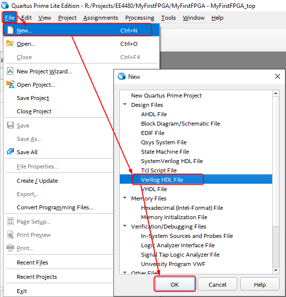
- After clicking OK, a new, empty file will open automatically. You can type your Verilog code in the Quartus Text Editor.
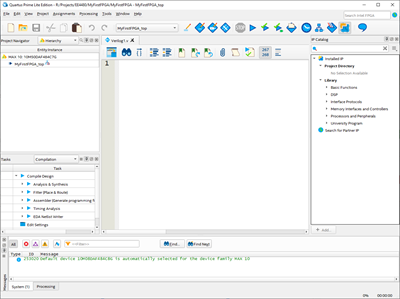
- Copy and paste the following code into your new Verilog file, then save it by selecting File ➤ Save. Keep the default file name and click Save in the Save As dialog box.
module MyFirstFPGA_top(SW, LEDR); input [9:0] SW; output [9:0] LEDR; assign in0 = SW[0]; assign in1 = SW[1]; assign sel = SW[2]; assign LEDR[0] = out; mux_2to1 mux21(.in0(in0), .in1(in1), .sel(sel), .out(out)); endmodule - Save the Verilog file. By default, the file name of the first Verilog file in the project will be the same as the top-level name, which you entered when creating a new project.
After creating the top-level module files, the next step is to go to the design sub-module — the 2-to-1 MUX.
- Select File ➤ New... from the Menu Bar.
Select the Verilog HDL File from the Design Files list and click OK.
- Copy and paste the following code into your new Verilog file, then save it by selecting File ➤ Save. Change the filename to mux_2to1.v and click Save.
module mux_2to1(in0, in1, sel, out);
    input  in0, in1, sel;
    output out;

    wire nsel;
    wire a0, a1;

    not not1(nsel, sel);
    and and1(a0, in0, nsel);
    and and2(a1, in1, sel);
    or  or1 (out, a0, a1);
endmodule
3. Compile the Design and RTL Viewer
Compile the Design and Check the RTL Viewer
Compile your Verilog code.
- Save all open files, and then partially compile the design by clicking the Processing ➤ Start Compilation ➤ Start Analysis & Elaboration, or click the
 icon.
icon.
- This will take a few minutes. You can check the progress (%), which is at the bottom right of the screen. Once it stops (progress to 100%), please look for any errors being displayed in the message box. If there were errors, try to fix them and try again. You may ignore any warnings that may appear at this time.
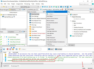
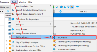
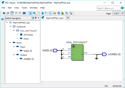
- After you perform a successful Analysis & Elaboration, you can view the design in the RTL Viewer, and you can view the hierarchy in the Project Navigator window. The Quartus RTL Viewer provides graphical representations of your design. To display the RTL Viewer, on the Tools menu, point to Netlist Viewers, and then click RTL Viewer.
Netlist Viewers provide two ways to display your final circuit: RTL Viewer and Technology Map Viewer.
- The RTL viewer shows what digital logic is implemented by your HDL code. It would be what you draw on paper if you were to design a digital circuit that satisfies your functional requirement.
- The Technology viewer shows how this digital circuit is implemented inside the FPGA. It depends on the technology inside the FPGA. For example, an OR gate is implemented as a simple LTU inside an FPGA. It shows how LUTs are used, which IOBs they use, and whether they use buffers on lines, etc.
4. Create a Test Bench File
Create a Test Bench File
For this tutorial, we want to test a simple 2-to-1 multiplexer circuit. We will run a simulation on the computer to test the logic and ensure there are no mistakes. This is faster than compiling and uploading to the FPGA board, and it is very powerful to be able to test the circuit without actually having to test it on hardware yet.
- Create a new file by going File ➤ New... ➤ Verilog HDL File, and click OK.

- Next, we will write the testbench code as shown below. Save the filename as "test_tb.v" file.
`timescale 1ns/1ps

module test_tb;

reg in0, in1, sel;
wire out;
wire [9:0] SW, LEDR;

MyFirstFPGA_top DUT(SW, LEDR);

assign SW[0] = in0;
assign SW[1] = in1;
assign SW[2] = sel;

assign out = LEDR[0];

initial begin
            sel = 0; in1 = 0; in0 = 0;
    #10     sel = 0; in1 = 0; in0 = 1;
    #10     sel = 0; in1 = 1; in0 = 0;
    #10     sel = 0; in1 = 1; in0 = 1;
    #10     sel = 1; in1 = 0; in0 = 0;
    #10     sel = 1; in1 = 0; in0 = 1;
    #10     sel = 1; in1 = 1; in0 = 0;
    #10     sel = 1; in1 = 1; in0 = 1;
    #10     $stop;
end

endmodule
Note: The testbench module contains no inputs or outputs and instantiates our mux module, which we want to test, calling it "DUT".
- Once you have finished writing everything, including the testbench, and everything compiles correctly, you can move to the next step.
5. Config and Launch Questa-Intel FPGA Simulation
Config Questa-Intel FPGA Simulation
Next, we need to set up the Simulation for the project.
- Click Assignments ➤ Settings ➤ EDA Tool Setting ➤ Simulation.
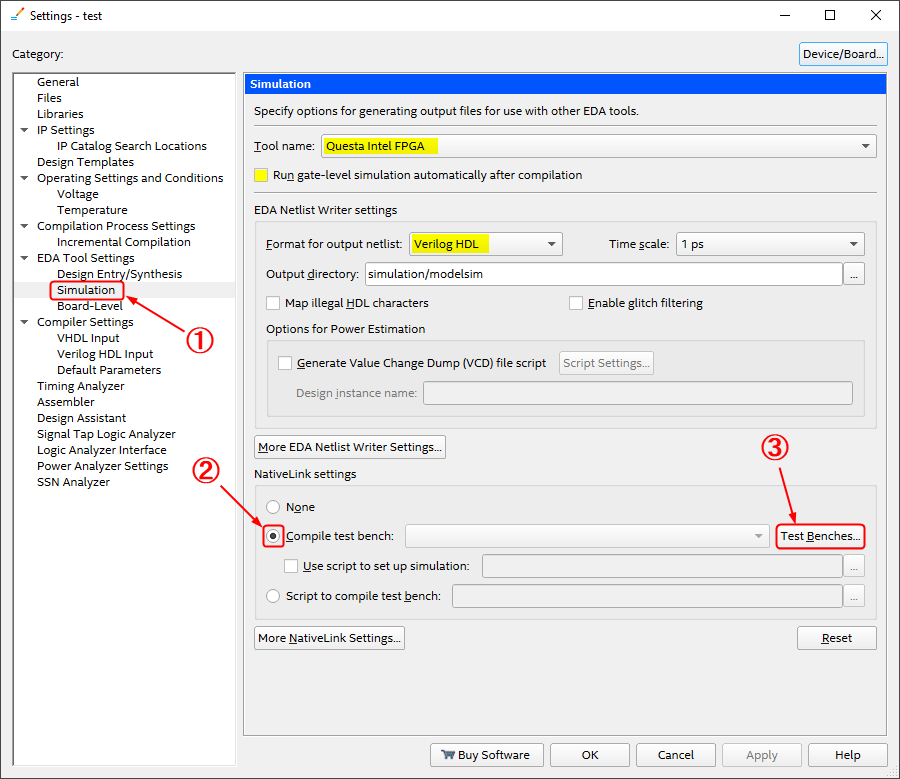
On the Simulation page, specify the following values for the options:
- Tool name: Questa Intel FPGA
- Run gate-level simulation automatically after compilation: unchecked
- Format for output netlist: Verilog HDL
- (2) Under NativeLink settings, select the Compile testbench option
- (3) Click the Test Benches... button
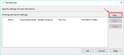
- On the Test Benches page, click the New option to create a new test bench.
- Specify test_tb as the Test bench name, and test_tb as the Top-level module in the test bench.
Check the Use test bench to perform VHDL timing simulation and set the DUT as the Design instance name in the test bench.
Under Test bench and simulation files, enter or select the test_tb.v file, click Add, then click OK.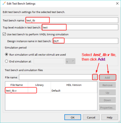
- The Test Benches dialog box displays the properties of the test benches in your project.
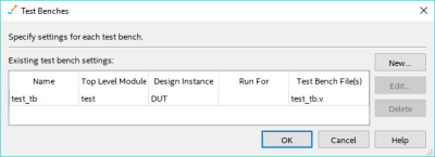
- Click OK to exit Test Benches and Settings dialogs.
Launch Simulation
To generate and run Questa-Intel FPGA Edition automation script from within the Altera Quartus Prime Standard Edition software, follow these steps:
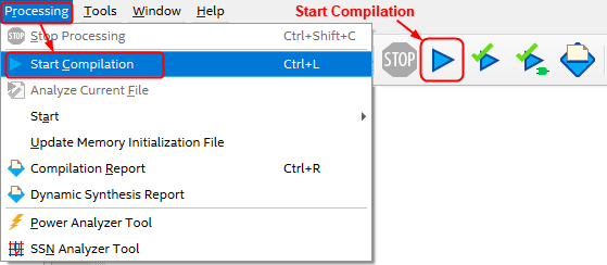
- Click Processing ➤ Start Compilation or click the
 icon to compile the design and generate the ".do" file. The Messages window indicates when compilation is complete.
- If there is no error, then click Tools ➤ Run Simulation Tool ➤ RTL Simulation. The Altera Quartus Prime Standard Edition software launches the Questa-Intel FPGA Edition simulator and simulates the test_tb.v file, according to your specifications in the Simulation settings.
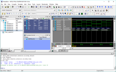
- On the Questa window, click the Wave panel. The simulation waveform ends at 80ns, as the testbench specifies. The Wave panel lists the in0, in1, sell, and out signals.
- If you got any problems, close Questa, fix the problems, and then run the Start Compilation again.
6. Assign Pins
Assign Pins
The DE10-Lite board has hardwired connections between the FPGA chip and onboard switches, seven-segment displays, and lights. To use those components, it is necessary to include in your Quartus project the correct pin assignments, which are given in your board’s user manual (Lesson KB 02: Intel DE10-Lite Board). For example, the DE10-Lite manual specifies that SW[0] is connected to the FPGA pin C10 and LEDR[0] is connected to pin A8. A good way to make the required pin assignments is to import into the Quartus software the pin assignment file for your board, which can be downloaded from here: DE10_Lite.qsf. Please download the QSF file and save it under your lab folder.
Importing Pin Assignments
With a project opened in Quartus, importing pin assignments are very simple. The detailed steps are as shown below.
- First, download DE10_Lite.qsf file.
- From the Menu Bar, select Assignments ➤ Import Assignments...
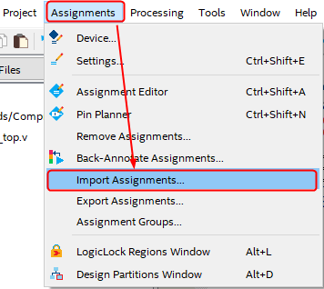
- Click ellipses next to Filename in the Import Assignments window that popped up.
Locate the file DE10_Lite.qsf, select the checkbox for the Copy existing assignment into <project>_top.qsf.bak before importing.
Then click the Advanced... button.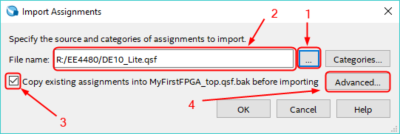
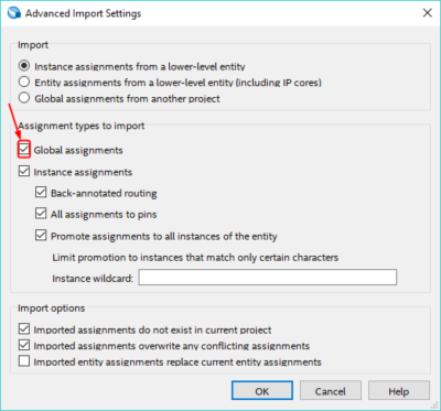
- In the Advanced Import Settings window, check the Global assignments, then click OK.
- Click OK again to import DE10_Lite.qsf into your project.
- Check the Pin Assignment
From the Menu Bar, select Assignment ➤ Assignment Editor. A complete list of pin assignments for the DE10-Lite board will be shown on the screen.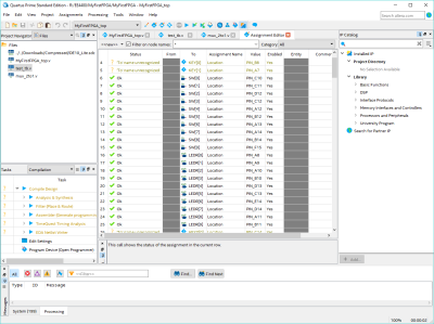
- Viewing Pin Assignments with the Pin Planner
To access the Pin Planner either click on the Pin Planner Icon, use the shortcut CTRL+SHIFT+N, or select the Pin Planner from the Assignments menu of the Quartus toolbar.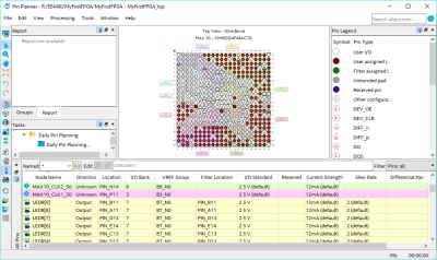
- Recompile the design by clicking Processing ➤ Start Compilation.
7. Program the FPGA board
Program the FPGA board
You must install the Altera USB-Blaster or Altera USB-Blaster II driver before you can use it to program devices with Quartus Prime software.
Driver Installation for Altera USB-Blaster (DE10-Lite Board)
The first time you plug in the USB-Blaster port, the Windows Found New Hardware dialog box prompts you to install the driver.
- Plug a USB cable into the USB-Blaster port and your PC. The Found New Hardware dialog box appears.
- Select Locate and install driver software (recommended)
- Select Don't search online.
- When prompted to insert the disc that came with your USB-Blaster, select "I don't have the disc." Show me other options.
- Select Browse my computer for driver software when you see the Windows couldn't find driver software for your device dialog box.
- Click Browse, and browse to the <Path to Quartus Prime installation>\Drivers\usb-blaster directory.
Note: Do not select the x32 or x64 directories. - Click OK.
- Select the Include subfolders option, and click Next.
- If you are prompted Windows can't verify the publisher of this driver software, select Install this driver software anyway in the Windows Security dialog box. The installation wizard guides you through the installation process.
- After the software for this device is successfully installed, a dialog box appears; click Close.
If no message appears when you plug the USB cable into the USB-Blaster Port and your PC, you may need to update the driver in Device Manager.
- Open Device Manager, then right-click the Unknown device under the Other devices branch.
- Select Update Driver Software.
- Select Browse my computer for driver software.
- Enter the location of the Quartus Prime software USB-Blaster driver files directory (C:\intelFPGA\<version>\quartus\drivers) in the Search for driver software in this location field.
- Click Next.
- Click Install in the Would you like to install this device software? Windows security dialog box.
- Close the Update Driver Software - Altera USB-Blaster (Unconfigured) successful installation notification. The Device Manager now shows a new branch called JTAG cables with an Altera USB-Blaster (Unconfigured) node.
- Open the Quartus Prime Programmer. Within a few seconds, the JTAG cable branch displays two nodes: Altera USB-Blaster II (JTAG interface) and Altera USB-Blaster II (System Console interface).
The following shows how to program the FPGA in JTAG mode, step by step.
- On the DE10-Lite board, plug the USB cable into the USB Blaster Port. Plug the other end of the USB cable into the computer.
- In the Quartus Prime window, click the Programmer button
 on the Toolbar, or select Tools ➤ Programmer from the Menu Bar to open the Programmer window.
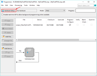
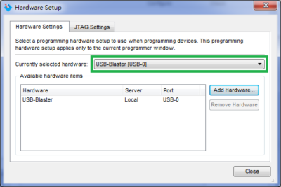
- The Hardware Setup... must be USB-Blaster [USB-xx]. If not, click the Hardware Setup... button and select USB-Blaster [USB-0] from the drop-down menu for Currently selected hardware. The mode should be set to JTAG. Click Close to close the window.
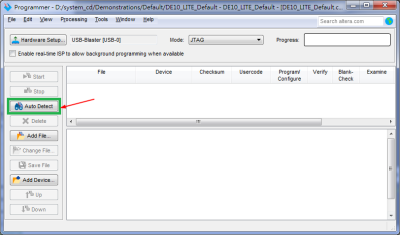
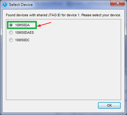
- If you can see an FPGA device on the Programmer screen, you can skip this step. Otherwise, click Auto Detect to detect all the devices on the JTAG chain, and select detected device associated with the board to 10M50DA. Click OK to detect the devices.
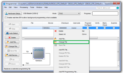
- Right-click on the FPGA device and click Change File to open the .sof file to be programmed.
- Click the Program/Configure check box, and then click the Start button to download the .sof file into the FPGA device.
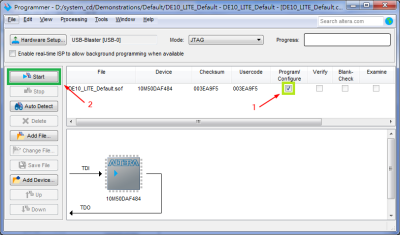
When the progress bar reaches 100%, programming is complete.
You can now test the program on the DE10-Lite board using the slide switches at the bottom of the board.
- SW0 is the single bit of input data.
- SW1 is the one bit of data for input1.
- SW2 is the selector input to the multiplexer.
- The multiplexer output is displayed on the first green LED above the slide switches on the DE10-Lite board.
