Tiva Lab 08: Interfacing Character LCD with Tiva LaunchPad
Objective
- Learn how to interface a character LCD module with a microcontroller in 4-bit mode
- Learn how to use ezTiva LIB to display a string on the LCD
Required Reading Materials
- Lesson 02: Data Types and Variables
- Lesson 03: Basic I/O Function
- Lesson 06: Loops
- Lesson 08: Add ezTiva Library into Your Project
- HD44780 Character LCD Module Datasheet
Overview
HD44780 based LCD modules are very popular among hobbyists because they are cheap and they can display characters. Besides they are very easy to interface with microcontrollers. In this lab, you will learn how to interface an HD44780 based character LCD to a TI Tiva LaunchPad. The interface requires 7 I/O lines of the TM4C microcontroller: 4 data lines and 3 control lines. You also will learn how to use ezTiva LIB in order to display information on the LCD module.
Components Required
 |
Character LCD Module | × 1 |
| 10 KΩ Potentiometer | × 1 | |
| Breadboard | × 1 | |
| Jumper Wires Ribbon Cable | × 1 | |
| Breadboard Power Supply Module | × 1 | |
| Power Adapter 9V/2A | × 1 |
Circuit Diagram
In this lab, a 16x2 character LCD module will be used and connected to the Tiva LaunchPad, as shown in the following diagram. The LCD module will be configured in 4-bit interfacing mode, so the data pin D[0]~D[3] on the LCD module will not be used. All the pins used to connect to the LCD module must be configured with the GPIO output direction.
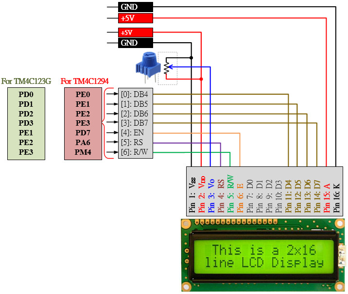
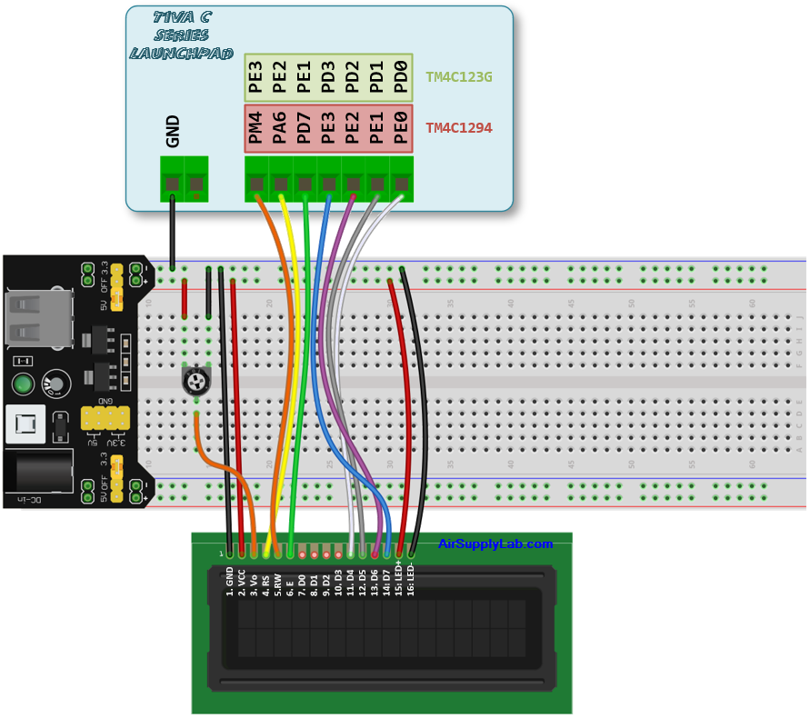
EK-TM4C123GXL LaunchPad
Pin configurations:
| Device | Port.Pin | Signal Type | PCTL | Direction | Drive Mode |
|---|---|---|---|---|---|
EK-TM4C1294XL LaunchPad
Pin configurations:
| Device | Port.Pin | Signal Type | PCTL | Direction | Drive Mode |
|---|---|---|---|---|---|
Procedures
- Create a new folder under the EE3450 folder and name it Lab07_CharLCD.
- Launch the Keil μVisio and create a new project. Save the project to the folder you created in the previous step and set the project name to Lab07_CharLCD.)
- Add the Common and ezTivaLIB folders to the Options for Target ➤ C/C++ ➤ include paths setting.
- Add ezTiva LIB (ez123GLIB.lib or ez1294LIB.lib) into your project, and increase the stack and heap size under the "startup_TM4cXXX.s (Startup)" setting. ()
Configurations
Write down the following configuration information in your lab report.
GPIO Initialization and Configuration
GPIO Initialization Configuration
Next, we need to configure all the GPIO ports and pins that are used in the design.
According to the pin connections, complete the following GPIO configurations for each port. Fills the pin field by the value below:
- 0: Clean the bit
- 1: Set the bit
- x: Do not change the bit
- d: Do not care
For both TM4C123GXL and TM4C1294XL LaunchPads, the Port C [3:0] are used for JTAG/SWD. Therefore, when you configure Port C, you have to use bitwise operators to make sure your new configuration settings do not affect the JTAG/SWD function (PC3 ~ PC0).
Most of GPIO pins are configured as GPIOs and tri-stated by default (GPIOPCTL = 0, CPIOAFSEL = 0, GPIODIR = 0, GPIOPUR = 0, GPIOPDR = 0, GPIOODR = 0)
- Enable Clock to the GPIO Modules (RCGCGPIO register)
TM4C123G: SYSCTL->RCGCGPIO |= (_PORTs); |= binary = hex
8 4 2 1 8 4 2 1 7 6 5 4 3 2 1 0 bit Port F Port E Port D Port C Port B Port A port 0 0 -
TM4C1294: SYSCTL->RCGCGPIO |= (_PORTs); |= binary = hex
After enabling the clock signal, check the PRGPIO register until the corresponding bit is set to 1.8 4 2 1 8 4 2 1 8 4 2 1 8 4 2 1 15 14 13 12 11 10 9 8 7 6 5 4 3 2 1 0 bit Port Q Port P Port N Port M Port L Port K Port J Port H Port G Port F Port E Port D Port C Port B Port A port 0 - - -
In Assembly:
            LDR     R0, =SYSCTL_PRGPIO_R
Wait4GPIO   LDR     R1, [R0]
            TST     R1, #(__)
            BEQ     Wait4GPIO
In c:
while ( (SYSCTL->PRGPIO & ____ ) != ____ ) {}; - Unlock Port
TM4C123G: PD7 and PF0 are locked after reset.
TM4C1294: PD7 and PE7 are locked after reset
If those pins are used in the design, they must be unlocked first. To unlock the port, 0x4C4F434B must be written into the GPIOLOCK register and uncommit it by setting the GPIOCR register.
8 4 2 1 8 4 2 1 7 6 5 4 3 2 1 0 bit Port Pin 7 Pin 6 Pin 5 Pin 4 - Pin 3 Pin 2 Pin 1 Pin 0 pin Value in Hex Register Value to Register - - = ➤ GPIO ->LOCK = 0x4C4F434B - - = ➤ GPIO ->CR - - = ➤ GPIO ->LOCK = 0x4C4F434B - - = ➤ GPIO ->CR
Convert above configuration into registers
- GPIO Analog Mode Select
If any pin is used as an Analog signal (check Signal Type field on table 1), the appropriate bit in AMSEL must be set.
- 0: Digital signal
- 1: Analog signal
8 4 2 1 8 4 2 1 7 6 5 4 3 2 1 0 bit Port Pin 7 Pin 6 Pin 5 Pin 4 - Pin 3 Pin 2 Pin 1 Pin 0 pin Value in Hex Register Value to Register - - = ➤ GPIO ->AMSEL - - = ➤ GPIO ->AMSEL - - = ➤ GPIO ->AMSEL - - = ➤ GPIO ->AMSEL - - = ➤ GPIO ->AMSEL - - = ➤ GPIO ->AMSEL - - = ➤ GPIO ->AMSEL - GPIO Port Control (PCTL)
The PCTL register is used to select the specific peripheral signal for each GPIO pin when using the alternate function mode.
- 0: GPIO
- 1~0xF: Check the GPIO Pins and Alternate Function table
8421 8421 8421 8421 8421 8421 8421 8421 31~28 27~24 23~20 19~16 15~12 11~8 7~4 3~0 bit Port Pin 7 Pin 6 Pin 5 Pin 4 - Pin 3 Pin 2 Pin 1 Pin 0 pin Value in Hex Register Value to Register - - = ➤ GPIO ->PCTL - - = ➤ GPIO ->PCTL - - = ➤ GPIO ->PCTL - - = ➤ GPIO ->PCTL - - = ➤ GPIO ->PCTL - - = ➤ GPIO ->PCTL - - = ➤ GPIO ->PCTL - GPIO Alternate Function Select (AFSEL)
Setting a bit in the AFSEL register configures the corresponding GPIO pin to be controlled by PCTL peripheral function.
- 0: General I/O
- 1: Pin connected to the digital function defined in the PCTL register
8 4 2 1 8 4 2 1 7 6 5 4 3 2 1 0 bit Port Pin 7 Pin 6 Pin 5 Pin 4 - Pin 3 Pin 2 Pin 1 Pin 0 pin Value in Hex Register Value to Register - - = ➤ GPIO ->AFSEL - - = ➤ GPIO ->AFSEL - - = ➤ GPIO ->AFSEL - - = ➤ GPIO ->AFSEL - - = ➤ GPIO ->AFSEL - - = ➤ GPIO ->AFSEL - - = ➤ GPIO ->AFSEL - GPIO Pin Direction (DIR)
Set pin direction
- 0: Input pin
- 1: Output pin
8 4 2 1 8 4 2 1 7 6 5 4 3 2 1 0 bit Port Pin 7 Pin 6 Pin 5 Pin 4 - Pin 3 Pin 2 Pin 1 Pin 0 pin Value in Hex Register Value to Register - - = ➤ GPIO ->DIR - - = ➤ GPIO ->DIR - - = ➤ GPIO ->DIR - - = ➤ GPIO ->DIR - - = ➤ GPIO ->DIR - - = ➤ GPIO ->DIR - - = ➤ GPIO ->DIR - Internal Pull-Up Resistor (PUR), Pull-Down Resistor (PDR), and Open-Drain (ODR)
PUR: The pull-up control register
PDR: The pull-down control register
ODR: The open-drain control register
- 0: Disable
- 1: Enable
8 4 2 1 8 4 2 1 7 6 5 4 3 2 1 0 bit Port Pin 7 Pin 6 Pin 5 Pin 4 - Pin 3 Pin 2 Pin 1 Pin 0 pin Value in Hex Register Value to Register - - = ➤ GPIO -> - - = ➤ GPIO -> - - = ➤ GPIO -> - - = ➤ GPIO -> - - = ➤ GPIO -> - - = ➤ GPIO -> - - = ➤ GPIO -> - GPIO Digital Enable
Enables all the pins that are used in the design, including GPIO pins and alternate function pins.
- 0: Pin undriven
- 1: Enable pin
8 4 2 1 8 4 2 1 7 6 5 4 3 2 1 0 bit Port Pin 7 Pin 6 Pin 5 Pin 4 - Pin 3 Pin 2 Pin 1 Pin 0 pin Value in Hex Register Value to Register - - = ➤ GPIO ->DEN - - = ➤ GPIO ->DEN - - = ➤ GPIO ->DEN - - = ➤ GPIO ->DEN - - = ➤ GPIO ->DEN - - = ➤ GPIO ->DEN - - = ➤ GPIO ->DEN
Example Source Code
Copy the following example code to your main.c file.
Note: The example code is not yet complete. You must implement all functions following the lab instructions.
EK-TM4C123GXL LaunchPad
Keil C Sample Firmware Code
The following code does not complete, you need to finish the GPIO configurations.
#include <stdio.h>
#include <stdlib.h>
#include <stdbool.h>
#include <stdint.h>

#include "TM4C123GH6PM.h"
#include "MyDefines.h"
#include "ez123G.h"

void Setup_GPIO(void);

int main(void)
{
    PEZOBJ_LCD  lcd;                                // Declare an object for LCD module
    char        str[100];
    uint16_t    i = 0;

    Setup_GPIO();                                   // GPIO Configuration

    lcd = ezLCD_Create();                           // Creating a new Hardware LCD Object
    ezLCD_Connect_DataPort(lcd, _PORTD, ON_PIN_3_0);// Connecting DATA port on PortD[3:0]
    ezLCD_Connect_ENPin(lcd, _PORTE, _PIN1);        // Connecting EN pin on PortE[1]
    ezLCD_Connect_RSPin(lcd, _PORTE, _PIN2);        // Connecting RS pin on PortE[2]
    ezLCD_Connect_RWPin(lcd, _PORTE, _PIN3);        // Connecting RW pin on PortE[3]

    ezLCD_Start(lcd);                               // Starting lcd object
    ezLCD_LoadVerticalBargraphFonts(lcd);           // Load vertical bargraph fonts

    ezLCD_ClearDisplay(lcd);                        // Clear LCD display
    ezLCD_PrintString(lcd, "HELLO");                // Display string on LCD screen
    ezLCD_Position(lcd, 1,0);                       // Set display position at [1,0] (raw 1. col 0)
    ezLCD_PrintString(lcd, "TI Tiva 123G");         // Display string on LCD screen

    while (1){
        sprintf(str,"i = %d  ", i);
        ezLCD_Position(lcd, 0, 6);
        ezLCD_PrintString(lcd, str);

        ezLCD_DrawVerticalBG(lcd, 1, 15, 2, i%16);
        i++;
        timer_waitMillis(100);                      // Hardware timer delay for 100 ms
    }
}
//------------------------------------------------------------------------------
/*
Device      Port.Pins       DIR     DriveMode
LCD_RS
LCD_RW
LCD_E
LCD_D4
LCD_D5
LCD_D6
LCD_D7

Port ____
*/

void Setup_GPIO()
{
    // GPIO Initialization and Configuration
    // 1. Enable Clock to the GPIO Modules (SYSCTL->RCGCGPIO |= (_PORTs);)
    SYSCTL->RCGCGPIO |= (__);
    // allow time for clock to stabilize (SYSCTL->PRGPIO & (_PORTs))
    while ((SYSCTL->PRGPIO & (__)) != (__)) {};
    // 2. Unlock GPIO only PD7, PF0 on TM4C123G; PD7 on TM4C1294 (GPIOx->LOCK = 0x4C4F434B; and GPIOx->CR = _PINs;)
    // 3. Set Analog Mode Select bits for each Port (GPIOx->AMSEL = _PINs;)
    // 4. Set Port Control Register for each Port (GPIOx->PCTL = PMCn << _PTCL_PINn, check the PCTL table)
    // 5. Set Alternate Function Select bits for each Port (GPIOx->AFSEL = _PINs;)
    // 6. Set Output pins for each Port (Direction of the Pins: GPIOx->DIR = _PINs;)

    // 7. Set PUR bits (internal Pull-Up Resistor), PDR (Pull-Down Resistor), ODR (Open Drain) for each Port
    // 8. Set Digital ENable register on all port.pins (GPIOx->DEN = _PINs;)

}
EK-TM4C1294XL LaunchPad
Keil C Sample Firmware Code
The following code does not complete, you need to finish the GPIO configurations.
#include <stdio.h>
#include <stdlib.h>
#include <stdbool.h>
#include <stdint.h>

#include "TM4C1294NCPDT.h"
#include "MyDefines.h"
#include "ez1294.h"

void Setup_GPIO(void);

int main(void)
{
    PEZOBJ_LCD  lcd;                                // Declare an object for LCD module
    char        str[100];
    uint16_t    i = 0;

    Setup_GPIO();                                   // GPIO Configuration

    lcd = ezLCD_Create();                           // Creating a new Hardware LCD Object
    ezLCD_Connect_DataPort(lcd, _PORTE, ON_PIN_3_0);// Connecting DATA port on PortE[3:0]
    ezLCD_Connect_ENPin(lcd, _PORTD, _PIN7);        // Connecting EN pin on PortD[7]
    ezLCD_Connect_RSPin(lcd, _PORTA, _PIN6);        // Connecting RS pin on PortA[6]
    ezLCD_Connect_RWPin(lcd, _PORTM, _PIN4);        // Connecting RW pin on PortM[4]

    ezLCD_Start(lcd);                               // Starting lcd object
    ezLCD_LoadVerticalBargraphFonts(lcd);           // Load vertical bargraph fonts

    ezLCD_ClearDisplay(lcd);                        // Clear LCD display
    ezLCD_PrintString(lcd, "HELLO");                // Display string on LCD screen
    ezLCD_Position(lcd, 1,0);                       // Set display position at [1,0] (raw 1. col 0)
    ezLCD_PrintString(lcd, "TI Tiva 1294");         // Display string on LCD screen

    while (1){
        sprintf(str,"i = %d  ", i);
        ezLCD_Position(lcd, 0, 6);
        ezLCD_PrintString(lcd, str);

        ezLCD_DrawVerticalBG(lcd, 1, 15, 2, i%16);
        i++;
        timer_waitMillis(100);                      // Hardware timer delay for 100 ms
    }
}
//------------------------------------------------------------------------------
/*
Device      Port.Pins       DIR     DriveMode
LCD_RS
LCD_RW
LCD_E
LCD_D4
LCD_D5
LCD_D6
LCD_D7

Port ____
*/

void Setup_GPIO()
{
    // GPIO Initialization and Configuration
    // 1. Enable Clock to the GPIO Modules (SYSCTL->RCGCGPIO |= (_PORTs);)
    SYSCTL->RCGCGPIO |= (__);
    // allow time for clock to stabilize (SYSCTL->PRGPIO & (_PORTs))
    while ((SYSCTL->PRGPIO & (__)) != (__)) {};
    // 2. Unlock GPIO only PD7, PF0 on TM4C123G; PD7 on TM4C1294 (GPIOx->LOCK = 0x4C4F434B; and GPIOx->CR = _PINs;)
    GPIOD_AHB->LOCK = 0x4C4F434B;
    while ((GPIOD_AHB->LOCK & 0x01) == 0x01); // Unlocked when reading the GPIOx->LOCK = 0x4C4F434B; ==0x00
    *(((char*)GPIOD_AHB)+0x524) = 0xFF;          // Unload PD7

    // 3. Set Analog Mode Select bits for each Port (GPIOx->AMSEL = _PINs;  0=digital, 1=analog)
    // 4. Set Port Control Register for each Port (GPIOx->PCTL = PMCn << _PTCL_PINn, check the PCTL table)
    // 5. Set Alternate Function Select bits for each Port (GPIOx->AFSEL = _PINs;  0=regular I/O, 1=PCTL peripheral)
    // 6. Set Output pins for each Port (Direction of the Pins: GPIOx->DIR = _PINs;  0=input, 1=output)

    // 7. Set PUR bits (internal Pull-Up Resistor), PDR (Pull-Down Resistor), ODR (Open Drain) for each Port
    // 8. Set Digital ENable register on all port.pins (GPIOx->DEN = _PINs;)

}
Lab Experiments
Use your embedded board to solve the following problems and display the result on the character LCD module.
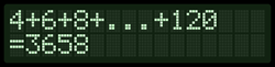
Exp #4.1: Calculate the Sum of Series
Do not directly show the answer on the screen. You have to use loop statements to get the answer.
Write a program in C to display the sum of a series on the LCD module. The series is: 4 + 6 + 8 + … + 120
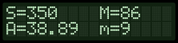
Exp #4.2: Calculate the Sum, Average, and Find the Maximum and Minimum Value from and Array
Write a program in C to calculate the sum, the average, and find the maximum and minimum values from an array, as shown below:
int array[]= {10, 35, 65, 43, 40, 86, 44, 9, 18};
You have to use loop statements to read each data from the array and then calculate the answers.
Display the results on the LCD module as shown below: (S: sum. M: maximum value, A: average, m: minimum value)