Lesson 01: PSoC 5LP Structures
The Infineon (Cypress) PSoC 5LP microcontroller offers a unique architecture that utilizes various structures to facilitate programming and optimize performance. Understanding these structures is crucial for effectively developing applications on this platform. Here's a detailed breakdown:
- Core Structures:
- ARM Cortex-M3 CPU: The PSoC 5LP core is built around a 32-bit Arm Cortex-M3 processor, which is responsible for executing your program code. This CPU interacts with other structures through its registers and buses.
- Memory Map: The PSoC5LP features a unified memory space, meaning both program code and data reside in the same Flash memory. This simplifies address calculations and eliminates the need for separate memory banks.
- Clock System: The microcontroller has multiple internal and external clock sources, allowing you to configure various peripherals and modules for efficient operation.
- Programmable Logic:
- Universal Digital Blocks (UDBs): These programmable blocks are the building blocks for custom digital logic. Through the PSoC Creator IDE, you can configure UDBs as gates, flip-flops, counters, state machines, or even simple CPUs.
- Digital Signal Processor (DSP): Integrated into the UDBs is a 24-bit fixed-point DSP block optimized for high-performance signal processing tasks. This allows you to implement algorithms like filtering, Fast Fourier Transforms (FFTs), and more.
- Analog Peripherals:
- Analog Front End (AFE): The PSoC 5LP includes a fully configurable AFE with programmable gain amplifiers (PGAs), analog-to-digital converters (ADCs), and digital-to-analog converters (DACs). This enables you to interface with various analog sensors and actuators.
- CapSense Touch Sensing: This technology allows you to create capacitive touch buttons and sliders without requiring dedicated touch-sensing hardware.
- Other Structures:
- Direct Memory Access (DMA) Controller: The DMA controller efficiently transfers data between memory and peripherals without involving the CPU, improving overall system performance.
- Interrupts: Interrupts allow peripherals and external events to signal the CPU and trigger specific actions, enabling efficient handling of asynchronous events.
- Timer/Counter/PWM Modules: These modules provide timing and pulse-width modulation (PWM) capabilities useful for driving LEDs, controlling motors, and performing real-time measurements.
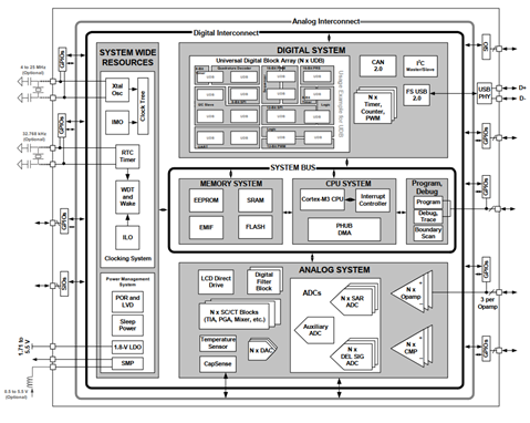
The following figure shows the major components of PSoC 5LP devices. The PSoC 5LP device uses the 32-bit ARM Cortex M3 core.
1.1 CPU System
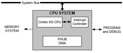
Figure 2: CPU System Block Diagram
Processor Core
The core of the PSoC 5LP CPU system is a 32-bit ARM Cortex-M3 processor with a three-stage pipeline capable of operating at speeds up to 80 MHz. This processor instruction set is the same as the Thumb-2 instruction set available on standard Cortex-M3 devices.
Interrupt Controller
- Nested Vectored Interrupt Controller (NVIC): This component enables low latency responses by allowing direct vectoring to the start of interrupt service routines, omitting the jump instruction required in other architectures.
- Advanced Features: The PSoC 5LP NVIC also includes enhanced interrupt handling capabilities like tail chaining, which optimizes stack management and reduces latency when dealing with multiple pending interrupts.
DMA (Direct Memory Access) Controller
Integrated into the CPU system, the DMA controller facilitates data exchange between peripherals without CPU intervention, thereby conserving power and freeing the CPU to enhance firmware algorithm performance.
Cache and Power Management
- Flash Cache with ECC (Error Correction Code): This feature minimizes the need for frequent flash memory access, contributing to lower system power consumption.
- Configurable Processor Speed: The processor's speed can be adjusted according to the application's needs, allowing for active power consumption optimization.
1.2 Memory System
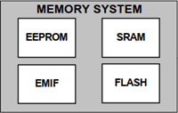
The PSoC5LP microcontroller boasts a diverse and flexible memory system catering to various program and data needs. Understanding these memory options is crucial for optimizing your project's performance and efficiency. Here's a detailed breakdown:
SRAM (Static RAM)
- Capacity: SRAM in PSoC 5LP devices varies in size but is usually smaller than flash memory, often in the range of 32 KB to 64 KB.
- Usage: This type of memory is used for temporary data storage during program execution. It's faster than flash memory, making it ideal for rapid access to data.
Flash Memory
- Size and Structure: The PSoC 5LP microcontroller has a large amount of flash memory, typically ranging from 64 KB to 256 KB. This non-volatile memory is used for storing the application code.
- Access Speed and Efficiency: Flash memory in PSoC 5LP is designed for high-speed access, and it often includes features like cache memory to enhance performance.
EEPROM (Electrically Erasable Programmable Read-Only Memory)
- Characteristics: PSoC 5LP microcontrollers often include a small amount of EEPROM, which is used for storing data that must be preserved between power cycles but is changed more frequently than the main program code.
- Advantages: EEPROM can be written at runtime, providing data storage and retention flexibility.
The PSoC 5LP's memory system is designed to balance storage capacity, access speed, data retention, and power efficiency, making it suitable for a wide range of embedded applications.
1.3 System Wide Resources
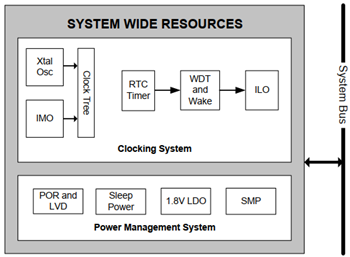
Figure: System Wide Resources Block Diagram
The PSoC 5LP microcontroller series, known for its versatility and performance, incorporates a comprehensive set of system-wide resources. These resources include sophisticated clocking systems, power management tools, and various other features that enhance the functionality and efficiency of the microcontroller. Here's a detailed overview of these resources:
Clocking System
- Internal Main Oscillator (IMO):
- The internal main oscillator (IMO) is the master clock base for the system, with 1% absolute accuracy at 3 MHz. The IMO can be configured to run from 3 MHz up to 74.7 MHz.
- The IMO is a configurable multi-frequency oscillator that can generate precise clock signals for the system. It's used as the primary clock source for the CPU and digital components.
- Internal Low-Speed Oscillator (ILO):
- The ILO provides three primary outputs, 1 kHz, 33 kHz, and 100 kHz.
- The ILO provides a low-power, low-frequency clock source for sleep and watchdog timers.
- Two External Clock Sources:
PSoC 5LP supports external clock sources, allowing for flexibility in system design. This is especially useful when specific clock frequencies or high precision are required.
- 4 to 25 MHz External Crystal Oscillator (ECO)
- 32.768 kHz External Crystal Oscillator for Real-Time Clock (RTC). The RTC in PSoC 5LP is used for time-keeping purposes, including date and time tracking.
- Watchdog Timer (WDT) and Wake-Up:
The WDT is designed to reset the system in case of software anomalies, ensuring system reliability. It can also be configured to wake the system from sleep modes.
Power Management System
- Power-On Reset (POR) and Low Voltage Detection (LVD):
POR ensures the system starts in a known state after power-up. LVD monitors the power supply voltage and triggers system actions to prevent improper operation during low-voltage conditions. - Sleep Power Modes:
The PSoC 5LP features various sleep modes that significantly reduce power consumption by shutting down microcontroller parts while retaining state information. - 1.8V Linear Dropout Regulator (LDO):
This regulator supplies a stable 1.8V output, essential for certain components within the microcontroller, even under varying input voltage conditions. - Selectable Mode Power (SMP): The SMP allows for dynamic power management by adjusting power consumption based on system activity, balancing performance and energy efficiency.
1.4 Digital System
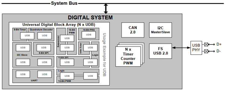
Figure: Digital System Block Diagram
The PSoC 5LP's digital system forms the foundation for its unique configurability and versatility. Understanding this crucial component is key to unlocking its full potential for your embedded projects. Here's a detailed breakdown of its key elements:
- Digital System Interconnect (DSI):
Imagine the DSI as a high-speed highway within the microcontroller. With incredible flexibility, it allows you to route digital signals from any peripheral, including UDBs, to any I/O pin. This opens up a world of possibilities for custom hardware configurations and data flow manipulation. - Universal Digital Blocks (UDBs):
Think of UDBs as the Lego bricks of the digital system. They are small, efficient building blocks packed with Programmable Array Logic (PAL) and Programmable Logic Device (PLD) functionality. You can configure them to implement various digital circuits, ranging from simple logic gates to complex state machines, enabling custom peripheral creation and adaptation. - State Machine Engine:
Embedded within each UDB is a dedicated state machine engine. This powerful tool allows you to define sequential logic and control operations within your UDB-based circuits, adding another layer of functionality and responsiveness. - Configurable Digital Blocks:
Beyond the flexible UDBs, PSoC 5LP offers pre-configured digital blocks for specific functions. These ready-made modules save you time and effort while ensuring reliable performance. Examples include:
- 16-bit Timer/Counter/PWM Blocks: Ideal for generating timing signals, controlling motors, and implementing dimming functions.
- I2C Slave/Master/Multi-Master: Provides versatile options for interfacing with various I2C devices.
- Full-Speed USB: Enables high-speed data transfer and storage with external devices like computers.
- CAN 2.0b: Facilitates robust communication with CAN-based devices in industrial and automotive applications.
- Benefits of the Digital System:
- Unmatched Configurability: Tailor the digital system to your specific needs, creating custom peripherals and optimizing logic flow.
- Improved Performance: UDBs and pre-configured blocks offer high speed and low power consumption compared to traditional microcontrollers.
- Reduced Development Time: Pre-built blocks and the DSI simplify circuit design and implementation.
- Scalability: Accommodate various application requirements with adaptable UDBs and diverse configurable blocks.
The PSoC 5LP's digital system empowers you to become an architect of your own hardware. By understanding its components and leveraging their strengths, you can unlock the true potential of this highly configurable microcontroller and bring your embedded projects to life with unparalleled flexibility and efficiency.
1.5 Analog System
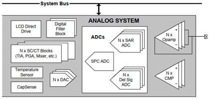
Figure: Analog System Block Diagram
The PSoC 5LP microcontroller, recognized for its versatility, includes a highly configurable analog system that complements its digital capabilities. This analog system is integral to the PSoC 5LP's functionality, offering a range of components that can be tailored to various applications. Below is a detailed overview of the PSoC 5LP's analog subsystem:
Core Features of the Analog System
- Highly Accurate Voltage Reference: The analog performance of the PSoC 5LP is based on a precise absolute voltage reference, ensuring accuracy and stability in analog operations.
- Analog Multiplexers (Muxes): These allow for flexible routing of analog signals within the chip, enhancing the configurability of the analog subsystem.
- Comparators: Used for comparing two voltages and outputting a digital signal based on the comparison.
- Voltage References: Provide stable reference voltages for various analog components.
- Operational Amplifiers (Opamps): These versatile amplifiers can boost signal strength, perform mathematical operations, and implement filters.
- Mixers: Enable the combination of different analog signals, useful in complex signal processing.
- Transimpedance Amplifiers (TIA): These specialized amplifiers are optimized for converting small currents from sensors into usable voltage signals.
- Analog-to-Digital Converters (ADC): Convert analog signals into digital data for processing.
- Digital-to-Analog Converters (DAC): Convert digital signals back into analog form.
- Digital Filter Block (DFB): Used for advanced signal processing, such as implementing IIR and FIR digital filters.
Key Analog Components
Analog-to-Digital and Digital-to-Analog Conversion
- Delta Sigma ADC: This advanced converter excels in precision and noise performance, ideal for capturing delicate analog signals from demanding sensors like temperature sensors or microphones. Think of it as a high-resolution camera capturing every detail of the analog world.
- Successive Approximation Register (SAR) ADC: Offering faster conversion speeds while still maintaining good accuracy, the SAR ADC is well-suited for applications requiring a balance between speed and precision, like audio processing or data acquisition. Think of it as a rapid-fire photographer capturing the dynamic movements of the analog world.
- Digital Filter Block (DFB): This powerful tool allows you to digitally refine and manipulate the digitized analog signals from the ADCs. Imagine it as a post-processing studio, enhancing the clarity and removing unwanted noise from your captured analog data.
- Digital-to-Analog Converters (DACs): These convert digital data back into analog signals, enabling control of devices like actuators, LEDs, or audio speakers. Think of them as digital translators, giving your digital commands a voice in the analog world.
Additional Analog Subsystem Components
High-Flexibility and Versatility:
- GPIO Pin Interface: All GPIO pins can be configured to handle analog signals, allowing you to interface with up to 62 discrete analog signals seamlessly. Think of it as a universal language translator, enabling communication between the digital and analog worlds through any I/O port.
- Configurable SC/CT Blocks: These building blocks offer further flexibility, allowing you to implement custom analog functions like filters, amplifiers, and mixers using software configuration. Think of them as programmable Lego bricks for constructing unique analog circuits.
The PSoC 5LP's analog system is a playground for analog creativity and precision. By delving into its depths, you equip yourself with the tools to translate the whispers of the analog world into actionable digital data and translate your digital commands into tangible real-world effects. Remember, experimentation and a deep understanding of the building blocks are key to unleashing the full potential of this versatile analog system.
1.6 Program/Debug
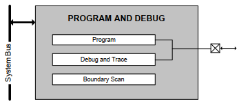
Figure: Program and Debug Block Diagram
The PSoC 5LP microcontroller series offers comprehensive program and debug capabilities, utilizing standard interfaces and advanced features. These functionalities are crucial for efficient development and troubleshooting of applications. Here’s a detailed look at the programming and debugging features of the PSoC 5LP:
Programming and Debug Interfaces
- JTAG (Joint Test Action Group):
- Type: 4-wire interface
- Usage: The industry-standard JTAG interface provides comprehensive debugging capabilities, including access to registers, memory, and setting breakpoints.
- Serial Wire Debug (SWD):
- Type: 2-wire interface.
- Functionality: A more lightweight alternative to JTAG, SWD uses fewer pins but still offers essential debugging functionalities.
- Single Wire Viewer (SWV):
- Type: 1-wire interface.
- Purpose: This "printf-style" debug option allows you to view variables and debug messages through a single pin, which is ideal for situations where pin constraints are tight.
- Combination with SWD: By combining SWD and SWV, a full debugging interface can be implemented with just three pins, optimizing the balance between functionality and hardware simplicity.
Advanced Debugging Features
The PSoC 5LP goes beyond basic debugging with these advanced features:
- On-chip Breakpoints: Set breakpoints directly in the microcontroller's memory, allowing you to pause program execution at specific points for detailed analysis.
- Instruction and Data Trace Memory: Analyze the program's execution flow by capturing instructions and data accessed during runtime.
- Flash Patch Breakpoint: Change instruction code on the fly without reprogramming the entire Flash memory, ideal for quick fixes and iterative development.
- Fast "printf"-style Debugging: Leverage the Trace Port Interface Unit (TPIU) for high-speed data transfers, enabling near real-time feedback through SWV for efficient debugging.
- Clock Cycle Counting: Accurately measure program execution time and identify performance bottlenecks.
- Data Watchpoint and Trace (DWT) Features: Set watchpoints on specific memory locations or data values to detect unexpected changes and debug memory-related issues.
- JTAG Scan Chains: Utilize JTAG for board-level testing and connecting multiple PSoC devices in a chain for debugging larger systems.
Compatibility and Versatility
- Support for Various Hardware Solutions: The PSoC 5LP can be debugged or programmed using a range of hardware tools, both from Cypress and third-party vendors.
- Flexibility: These debugging capabilities provide developers with the flexibility to implement a wide range of debugging strategies, from basic code observation to advanced performance analysis.
Integration in the Development Process
- Efficient Development: The advanced program and debug features of the PSoC 5LP facilitate rapid development and troubleshooting, making it easier to bring robust and reliable applications to market quickly.
- Application Versatility: With these comprehensive debugging capabilities, the PSoC 5LP is suitable for a wide range of applications, from simple control tasks to complex, interconnected systems.
In summary, the PSoC 5LP’s programming and debugging features provide developers with powerful and versatile tools essential for the efficient development and maintenance of sophisticated embedded systems.
