Lab 03: Single-Cycle MIPS Datapath
Objective
This lab aims to implement the first half of a simple processor that runs a subset of the MIPS ISA. This processor includes an instruction fetch unit, instruction decode logic, execution units, memory access, and data write-back unit, similar to a real processor. All students will implement the same datapath, and it is recommended to learn from classmates' experiences and apply that knowledge to your design.
Required Reading Materials
- MIPS32 Instruction Set Architecture
- Computer Organization and Design - The Hardware/Software Interface 5th Edition (ISDN: 978-0-12-407726-3): Chapter 4.3, 4.4
Specifications of the MIPS CPU
Instruction Set Supported
The machine supports all MIPS instructions specified in Lab 1, excluding those related to multiplication and division: DIV, DIVU, MFHI, MFLO, MTHI, MTLO, MULT, and MULTU. As shown in the following table, there are 45 MIPS instructions that the machine supports.
| ADD | ADDU | ADDI | ADDIU | AND | ANDI | BEQ |
| BNE | ||||||
| DIV | DIVU | J | JAL | JALR | JR | LB |
| LBU | LH | LHU | LUI | LW | MFHI | MFLO |
| MTHI | MTLO | MULT | MULTU | NOR | OR | ORI |
| SB | SH | SLL | SLLV | SLT | SLTI | SLTIU |
| SLTU | SRA | SRAV | SRL | SRLV | SUB | SUBU |
| SW | SYSCALL | XOR | XORI |
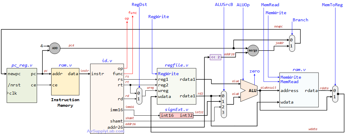
Circuit Diagram

In this lab, you will build the schematic provided above by implementing some modules and wiring up all components accordingly. To begin, create a new project in Quartus Prime and target the MAX10-Lite board, as done in the previous lab.
You are going to implement all modules in your project.